ZHCS360F July 2012 – November 2020 TPS54020
PRODUCTION DATA
- 1 特性
- 2 应用
- 3 说明
- 4 Revision History
- 5 Description (Continued)
- 6 Pin Configuration and Functions
- 7 Specifications
-
8 Detailed Description
- 8.1 Overview
- 8.2 Functional Block Diagram
- 8.3
Feature Description
- 8.3.1 Fixed Frequency PWM Control
- 8.3.2 Input Voltage and Power Input Voltage Pins (VIN and PVIN)
- 8.3.3 Voltage Reference (VREF)
- 8.3.4 Adjusting the Output Voltage
- 8.3.5 Safe Start-up into Prebiased Outputs
- 8.3.6 Error Amplifier
- 8.3.7 Slope Compensation
- 8.3.8 Enable and Adjusting Undervoltage Lockout
- 8.3.9 Adjustable Switching Frequency and Synchronization (RT/CLK)
- 8.3.10 Soft-Start (SS) Sequence
- 8.3.11 Power Good (PWRGD)
- 8.3.12 Bootstrap Voltage (BOOT) and Low Dropout Operation
- 8.3.13 Sequencing (SS)
- 8.3.14 Output Overvoltage Protection (OVP)
- 8.3.15 Overcurrent Protection
- 8.3.16 Thermal Shutdown
- 8.4 Device Functional Modes
-
9 Application and Implementation
- 9.1 Application Information
- 9.2
Typical Application
- 9.2.1 Design Requirements
- 9.2.2
Detailed Design Procedure
- 9.2.2.1 Custom Design With WEBENCH® Tools
- 9.2.2.2 Operating Frequency
- 9.2.2.3 Output Inductor Selection
- 9.2.2.4 Output Capacitor Selection
- 9.2.2.5 Input Capacitor Selection
- 9.2.2.6 Soft-Start Capacitor Selection
- 9.2.2.7 Bootstrap Capacitor Selection
- 9.2.2.8 Undervoltage Lockout Set Point
- 9.2.2.9 Output Voltage Feedback Resistor Selection
- 9.2.2.10 Compensation Component Selection
- 9.2.3 Application Curves
- 10Power Supply Recommendations
- 11Layout
- 12Device and Documentation Support
- 13Mechanical, Packaging, and Orderable Information
8.4.4 Eco-mode Light-Load Efficiency Operation
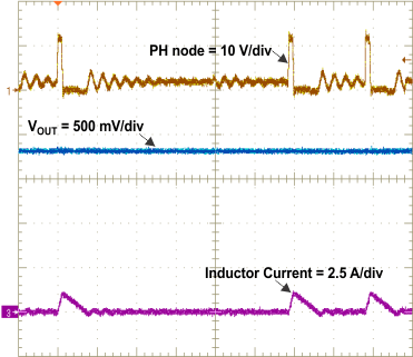
The TPS54020 operates in pulse skip mode (see Figure 8-9) at light-load currents to improve efficiency by reducing switching, gate drive, and circulating current losses. When the output voltage is in regulation and the peak switch current at the end of any switching cycle remains below the pulse skipping current threshold, the device enters pulse skip mode. This current threshold is the current level corresponding to a nominal COMP voltage of 270 mV.
When in pulse skip mode, the device clamps the COMP pin voltage to 270 mV and inhibits the high-side MOSFET. Further decreases in load current cannot drive the COMP pin below this clamp voltage level.
When the device is not switching while in pulse skip mode, the output voltage tends to decay. As the voltage control loop compensates for the falling output voltage, the COMP pin voltage begins to rise. At this time, the device enables the high-side MOSFET, and a switching pulse initiates on the next clock cycle. The COMP pin voltage sets the peak switch current. The output voltage re-charges to the regulation set point value, and then the demand for peak switch current will decrease. Eventually, the COMP pin voltage once again falls below the pulse skip mode threshold, at which time the device again enters pulse skip mode.
Bias circuits in the BOOT regulator and high-side MOSFET gate drive both return bias current out from the PH pin. While this current is small and in the range of 150 µA (nominal), during very light load conditions, it is possible that the output voltage rises above the desired output voltage setpoint due to this current. If the application design anticipates that system loads can fall below this current level, it is recommended to add a fixed resistor load to the design that dissipates this current. An easy implementation of this fixed load can be achieved with the feedback voltage divider resistors. The recommendation is to use a lower divider resistor value of 2.5 kΩ or lower in this case, and this lower divider resistor should be installed even when the output voltage setpoint is 0.6 V.
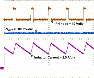
 Figure 8-7 TPS54020 in Continuous Conduction Mode
 Figure 8-9 TPS54020 in Pulse Skipping Mode
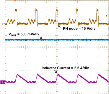
 Figure 8-8 TPS54020 in Discontinuous Conduction Mode