ZHCSOL9B March 2013 – August 2021 TPS53511
PRODUCTION DATA
- 1 特性
- 2 应用
- 3 说明
- 4 Revision History
- 5 Pin Configuration and Functions
- 6 Specifications
- 7 Detailed Description
- 8 Application and Implementation
- 9 Power Supply Recommendations
- 10Layout
- 11Device and Documentation Support
- 12Mechanical, Packaging, and Orderable Information
8.2.2.1 Output Inductor Selection
The value of the output filtering inductor determines the magnitude of the current ripple, which also affects the output voltage ripple for a certain output capacitance value. Increasing the inductance value reduces the ripple current, and thus, results in reduced conduction loss and output ripple voltage. Alternatively, low inductance value is needed due to the demand of low profile and fast transient response. Therefore, it is important to obtain a compromise between the low ripple current and low inductance value.
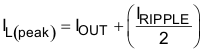
In practical application, the peak-to-peak current ripple is usually designed to be between 1/4 to1/2 of the rated load current. Since the magnitude of the current ripple is determined by inductance value, switching frequency, input voltage and output voltage, the required inductance value for a certain required ripple ∆I is shown in Equation 3. Also, the chosen inductor should be rated for the peak current calculated from Equation 4.
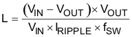
where
- VIN is the input voltage.
- VOUT is the output voltage.
- IRIPPLE is the required current ripple.
- ƒSW is the switching frequency.
For this design example, the inductance value is selected to provide approximately 30% peak-to-peak ripple current at maximum load. For this design, a nearest standard value was chosen: 3.3 µH. For 3.3 µH, the calculated peak current is 1.71 A.