ZHCSQC2A November 2015 – July 2022 TPS51216-EP
PRODUCTION DATA
- 1 特性
- 2 应用
- 3 说明
- 4 Revision History
- 5 说明(续)
- 6 Pin Configuration and Functions
- 7 Specifications
- 8 Detailed Description
- 9 Application and Implementation
- 10Power Supply Recommendations
- 11Layout
- 12Device and Documentation Support
- 13Mechanical, Packaging, and Orderable Information
9.1.1 D-CAP Mode
Figure 9-1 shows a simplified model of D-CAP mode architecture.
 Figure 9-1 Simplified D-CAP Model
The VDDQSNS voltage is compared with REFIN voltage. The PWM comparator creates a set signal to turn on the high-side MOSFET. The gain and speed of the comparator is high enough to maintain the voltage at the beginning of each on-cycle (or the end of each off-cycle) to be substantially constant. The DC output voltage monitored at VDDQ may have line regulation due to ripple amplitude that slightly increases as the input voltage increase. The D-CAP mode offers flexibility on output inductance and capacitance selections and provides ease-of-use with a low external component count. However, it requires a sufficient amount of output ripple voltage for stable operation and good jitter performance.
The requirement for loop stability is simple and is described in Equation 1. The 0-dB frequency, ƒ0 defined in Equation 1, is recommended to be lower than 1/3 of the switching frequency to secure proper phase margin.
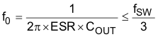
where
- ESR is the effective series resistance of the output capacitor
- COUT is the capacitance of the output capacitor
- ƒsw is switching frequency
Jitter is another attribute caused by signal-to-noise ratio of the feedback signal. One of the major factors that determine jitter performance in D-CAP mode is the down-slope angle of the VDDQSNS ripple voltage. Figure 9-2 shows, in the same noise condition, a jitter is improved by making the slope angle larger.
 Figure 9-2 Ripple Voltage Slope and Jitter Performance
For a good jitter performance, use the recommended down slope of approximately 20 mV per switching period as shown in Figure 9-2 and Equation 2.
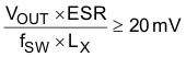
where
- VOUT is the VDDQ output voltage
- LX is the inductance