ZHCSQC2A November 2015 – July 2022 TPS51216-EP
PRODUCTION DATA
- 1 特性
- 2 应用
- 3 说明
- 4 Revision History
- 5 说明(续)
- 6 Pin Configuration and Functions
- 7 Specifications
- 8 Detailed Description
- 9 Application and Implementation
- 10Power Supply Recommendations
- 11Layout
- 12Device and Documentation Support
- 13Mechanical, Packaging, and Orderable Information
9.1.5 VDDQ Overcurrent Protection
The VDDQ SMPS has cycle-by-cycle overcurrent limiting protection. The inductor current is monitored during the off-state using the low-side MOSFET RDS(on) and the controller maintains the off-state while the voltage across the low-side MOSFET is larger than the overcurrent trip level. The current monitor circuit inputs are PGND and SW pins so that those should be properly connected to the source and drain terminals of low-side MOSFET. The overcurrent trip level, VTRIP, is determined by Equation 4.

where
- RTRIP is the value of the resistor connected between the TRIP pin and GND
- ITRIP is the current sourced from the TRIP pin. ITRIP is 10 μA typically at room temperature, and has 4700 ppm/°C temperature coefficient to compensate the temperature dependency of the low-side MOSFET RDS(on).
Because the comparison is done during the off-state, VTRIP sets the valley level of the inductor current. The load current OCL level, IOCL, can be calculated by considering the inductor ripple current as shown in Equation 5.
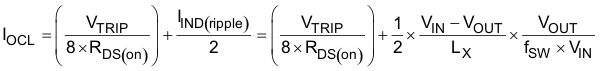
where
- IIND(ripple) is inductor ripple current
In an overcurrent condition, the current to the load exceeds the current to the output capacitor, thus the output voltage tends to fall down. Eventually, it crosses the undervoltage protection threshold and shuts down.