ZHCSSZ6F august 2008 – june 2020 TPS40210-Q1 , TPS40211-Q1
PRODUCTION DATA
- 1
- 1 特性
- 2 应用
- 3 说明
- 5
- 4 Revision History
- 5 Pin Configuration and Functions
- 6 Specifications
-
7 Detailed Description
- 7.1 Overview
- 7.2 Functional Block Diagram
- 7.3
Feature Description
- 7.3.1 Minimum On-Time and Off-Time Considerations
- 7.3.2 Current Sense and Overcurrent
- 7.3.3 Current Sense and Subharmonic Instability
- 7.3.4 Current Sense Filtering
- 7.3.5 Soft Start
- 7.3.6 BP Regulator
- 7.3.7 Shutdown (DIS/ EN Pin)
- 7.3.8 Control Loop Considerations
- 7.3.9 Gate Drive Circuit
- 7.3.10 TPS40211-Q1
- 7.4 Device Functional Modes
-
8 Application and Implementation
- 8.1 Application Information
- 8.2
Typical Application
- 8.2.1 Design Requirements
- 8.2.2
Detailed Design Procedure
- 8.2.2.1 Duty Cycle Estimation
- 8.2.2.2 Inductor Selection
- 8.2.2.3 Rectifier Diode Selection
- 8.2.2.4 Output Capacitor Selection
- 8.2.2.5 Input Capacitor Selection
- 8.2.2.6 Current Sense and Current Limit
- 8.2.2.7 Current Sense Filter
- 8.2.2.8 Switching MOSFET Selection
- 8.2.2.9 Feedback Divider Resistors
- 8.2.2.10 Error Amplifier Compensation
- 8.2.2.11 R-C Oscillator
- 8.2.2.12 Soft-Start Capacitor
- 8.2.2.13 Regulator Bypass
- 8.2.3 Application Curves
- 9 Power Supply Recommendations
- 10Layout
- 11Device and Documentation Support
- 12Mechanical, Packaging, and Orderable Information
7.4.2 Synchronizing the Oscillator
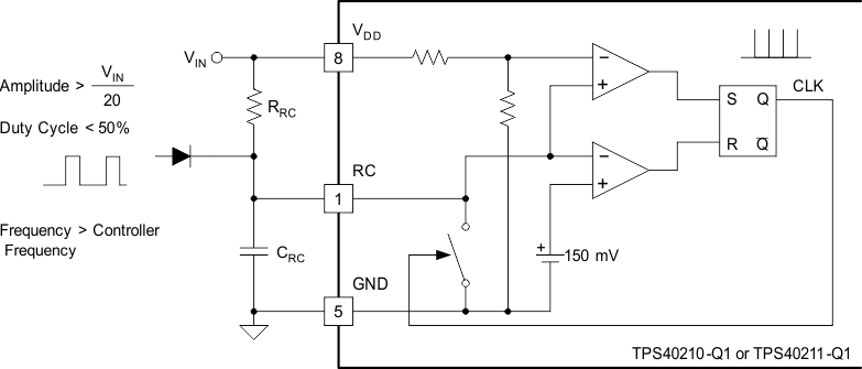
The TPS40210-Q1 and TPS40211-Q1 devices can be synchronized to an external clock source. Figure 7-9 shows the functional diagram of the oscillator. When synchronizing the oscillator to an external clock, the RC pin must be pulled below 150 mV for 20 ns or more. The external clock frequency must be higher than the free running frequency of the converter as well. When synchronizing the controller, if the RC pin is held low for an excessive amount of time, erratic operation can occur. The maximum amount of time that the RC pin should be held low is 50% of a nominal output pulse, or 10% of the period of the synchronization frequency.
Under circumstances where the duty cycle is less than 50%, a Schottky diode connected from the RC pin to an external clock can be used to synchronize the oscillator. The cathode of the diode is connected to the RC pin. The trip point of the oscillator is set by an internal voltage divider to be 1/20 of the input voltage. The clock signal must have an amplitude higher than this trip point. When the clock goes low, it allows the reset current to restart the RC ramp, synchronizing the oscillator to the external clock. This provides a simple single-component method for clock synchronization.
 Figure 7-9 Oscillator Functional Diagram
 Figure 7-10 Diode Connected Synchronization