ZHCSSZ6F august 2008 – june 2020 TPS40210-Q1 , TPS40211-Q1
PRODUCTION DATA
- 1
- 1 特性
- 2 应用
- 3 说明
- 5
- 4 Revision History
- 5 Pin Configuration and Functions
- 6 Specifications
-
7 Detailed Description
- 7.1 Overview
- 7.2 Functional Block Diagram
- 7.3
Feature Description
- 7.3.1 Minimum On-Time and Off-Time Considerations
- 7.3.2 Current Sense and Overcurrent
- 7.3.3 Current Sense and Subharmonic Instability
- 7.3.4 Current Sense Filtering
- 7.3.5 Soft Start
- 7.3.6 BP Regulator
- 7.3.7 Shutdown (DIS/ EN Pin)
- 7.3.8 Control Loop Considerations
- 7.3.9 Gate Drive Circuit
- 7.3.10 TPS40211-Q1
- 7.4 Device Functional Modes
-
8 Application and Implementation
- 8.1 Application Information
- 8.2
Typical Application
- 8.2.1 Design Requirements
- 8.2.2
Detailed Design Procedure
- 8.2.2.1 Duty Cycle Estimation
- 8.2.2.2 Inductor Selection
- 8.2.2.3 Rectifier Diode Selection
- 8.2.2.4 Output Capacitor Selection
- 8.2.2.5 Input Capacitor Selection
- 8.2.2.6 Current Sense and Current Limit
- 8.2.2.7 Current Sense Filter
- 8.2.2.8 Switching MOSFET Selection
- 8.2.2.9 Feedback Divider Resistors
- 8.2.2.10 Error Amplifier Compensation
- 8.2.2.11 R-C Oscillator
- 8.2.2.12 Soft-Start Capacitor
- 8.2.2.13 Regulator Bypass
- 8.2.3 Application Curves
- 9 Power Supply Recommendations
- 10Layout
- 11Device and Documentation Support
- 12Mechanical, Packaging, and Orderable Information
8.2.2.8 Switching MOSFET Selection
The TPS40210-Q1 device drives a ground referenced N-channel FET. The RDS(on) and gate charge are estimated based on the desired efficiency target.

For a target of 95% efficiency with a 24-V input voltage at 2 A, maximum power dissipation is limited to 2.526 W. The main power dissipating devices are the MOSFET, inductor, diode, current sense resistor and the integrated circuit, the TPS40210-Q1 device.

This leaves 740 mW of power dissipation for the MOSFET. This can likely cause an SO-8 MOSFET to get too hot, so power dissipation is limited to 500 mW. Allowing half for conduction and half for switching losses, you can determine a target RDS(on) and QGS for the MOSFET by Equation 54 and Equation 55.
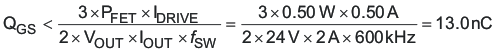
A target MOSFET gate-to-source charge of less than 13.0 nC is calculated to limit the switching losses to less than 250 mW.
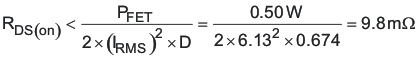
A target MOSFET RDS(on) of 9.8 mΩ is calculated to limit the conduction losses to less than 250 mW. Reviewing 30-V and 40-V MOSFETs, an Si4386DY 9-mΩ MOSFET is selected. A gate resistor was added per Equation 29. The maximum gate charge at Vgs = 8 V for the Si4386DY is 33.2 nC, this implies RG = 3.3 Ω.