ZHCSSZ6F august 2008 – june 2020 TPS40210-Q1 , TPS40211-Q1
PRODUCTION DATA
- 1
- 1 特性
- 2 应用
- 3 说明
- 5
- 4 Revision History
- 5 Pin Configuration and Functions
- 6 Specifications
-
7 Detailed Description
- 7.1 Overview
- 7.2 Functional Block Diagram
- 7.3
Feature Description
- 7.3.1 Minimum On-Time and Off-Time Considerations
- 7.3.2 Current Sense and Overcurrent
- 7.3.3 Current Sense and Subharmonic Instability
- 7.3.4 Current Sense Filtering
- 7.3.5 Soft Start
- 7.3.6 BP Regulator
- 7.3.7 Shutdown (DIS/ EN Pin)
- 7.3.8 Control Loop Considerations
- 7.3.9 Gate Drive Circuit
- 7.3.10 TPS40211-Q1
- 7.4 Device Functional Modes
-
8 Application and Implementation
- 8.1 Application Information
- 8.2
Typical Application
- 8.2.1 Design Requirements
- 8.2.2
Detailed Design Procedure
- 8.2.2.1 Duty Cycle Estimation
- 8.2.2.2 Inductor Selection
- 8.2.2.3 Rectifier Diode Selection
- 8.2.2.4 Output Capacitor Selection
- 8.2.2.5 Input Capacitor Selection
- 8.2.2.6 Current Sense and Current Limit
- 8.2.2.7 Current Sense Filter
- 8.2.2.8 Switching MOSFET Selection
- 8.2.2.9 Feedback Divider Resistors
- 8.2.2.10 Error Amplifier Compensation
- 8.2.2.11 R-C Oscillator
- 8.2.2.12 Soft-Start Capacitor
- 8.2.2.13 Regulator Bypass
- 8.2.3 Application Curves
- 9 Power Supply Recommendations
- 10Layout
- 11Device and Documentation Support
- 12Mechanical, Packaging, and Orderable Information
7.3.1 Minimum On-Time and Off-Time Considerations
The TPS40210-Q1 device has a minimum off-time of approximately 200 ns and a minimum on-time of 300 ns. These two constraints place limitations on the operating frequency that can be used for a given input-to-output conversion ratio. See Figure 6-2 for the maximum frequency that can be used for a given duty cycle.
The duty cycle at which the converter operates is dependent on the mode in which the converter is running. If the converter is running in discontinuous-conduction mode, the duty cycle varies with changes to the load much more than it does when running in continuous-conduction mode.
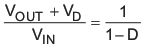
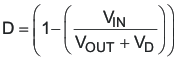
In continuous-conduction mode, the duty cycle is related primarily to the input and output voltages.
In discontinuous-conduction mode, the duty cycle is a function of the load, input and output voltages, inductance, and switching frequency.
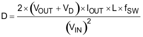
All converters using a diode as the freewheeling or catch component have a load current level at which they transition from discontinuous conduction to continuous conduction. This is the point at which the inductor current falls to zero. At higher load currents, the inductor current does not fall to zero but remains flowing in a positive direction and assumes a trapezoidal wave shape as opposed to a triangular wave shape. This load boundary between discontinuous conduction and continuous conduction can be found for a set of converter parameters as shown in Equation 4.
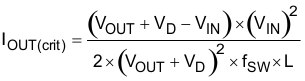
For loads higher than the result of Equation 4, the duty cycle is given by Equation 2, and for loads less than the results of Equation 4, the duty cycle is given Equation 3. For Equation 1 through Equation 4, the variable definitions are as follows:
- VOUT is the output voltage of the converter in V.
- VD is the forward conduction voltage drop across the rectifier or catch diode in V.
- VIN is the input voltage to the converter in V.
- IOUT is the output current of the converter in A.
- L is the inductor value in H.
- fSW is the switching frequency in Hz.