SBVS193D June 2012 – July 2015 TPS3831 , TPS3839
PRODUCTION DATA.
- 1 Features
- 2 Applications
- 3 Description
- 4 Revision History
- 5 Device Options
- 6 Pin Configuration and Functions
- 7 Specifications
- 8 Detailed Description
- 9 Applications and Implementation
- 10Power Supply Recommendations
- 11Layout
- 12Device and Documentation Support
- 13Mechanical, Packaging, and Orderable Information
封装选项
机械数据 (封装 | 引脚)
散热焊盘机械数据 (封装 | 引脚)
- DQN|4
订购信息
9 Applications and Implementation
NOTE
Information in the following applications sections is not part of the TI component specification, and TI does not warrant its accuracy or completeness. TI’s customers are responsible for determining suitability of components for their purposes. Customers should validate and test their design implementation to confirm system functionality.
9.1 Application Information
Low operating voltage and threshold options make the TPS383x devices well-suited for monitoring single-cell, alkaline-battery applications.
9.2 Typical Application
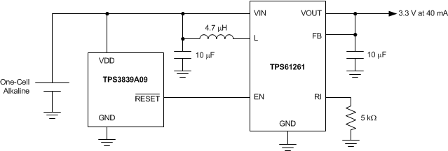
Figure 15 shows the TPS3839A09 used to disable a boost converter when the cell voltage reaches 0.9 V, which is the end of the discharge voltage for a single alkaline battery cell. When the cell voltage reaches 0.9 V, the TPS61261 enable pin is driven low. This setting disables the TPS61261 and places it in a low-current shutdown state. The combination of the TPS3839 and TPS61261 devices consumes only 250 nA (typical) from the discharged battery.
9.2.1 Design Requirements
Table 1 lists the design requirements for Figure 15.
Table 1. Design Requirements and Results
| DESIGN REQUIREMENTS | DESIGN RESULT | ||
|---|---|---|---|
| TPS3839A09 | TPS61261 | COMBINED | |
| Input voltage range of 0.9 V to 1.7 V | 0.9 V to 6.5 V | 0.8 V to 4 V | 0.9 V to 4 V |
| Shutdown current < 3 µA | 0.5 μA (maximum) | 1.5 μA (maximum) | 2.0 μA (maximum) |
| Output voltage of 3.3 V | N/A | 3.3 V | 3.3 V |
| Output current of 50 mA | N/A | 100 mA | 100 mA |
| Switching frequency ≥ 1 MHz | N/A | 2.5 MHz | 2.5 MHz |
9.2.2 Detailed Design Procedure
9.2.2.1 Input Capacitor
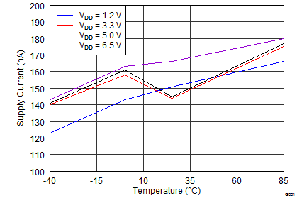
The TPS383x devices use a unique sampling scheme to maintain an extremely low average quiescent current of 150 nA. The TPS383x devices typically consume only approximately 100 nA of dc current. However, this current rises to approximately 15 µA for about 200 µs when the TPS383x devices sample the input voltage. If the source impedance back to the supply voltage is high, then the additional current during sampling may trigger a false reset as a result of the apparent voltage drop at VDD. For applications with high-impedance input supplies (including trace impedance), TI recommends adding a small 0.1-µF bypass capacitor near the TPS3839 VDD pin. This bypass capacitor effectively keeps the average current at 150 nA and reduces the effects of a high-impedance voltage source.
9.2.2.2 Bidirectional Reset Pins
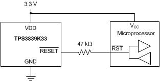
Some devices have bidirectional reset pins that act both as an input and an output. For applications where the TPS383x devices drive a bidirectional reset pin, place a series resistor between the TPS383x output and the reset pin to protect against excessive current flow when both the TPS383x devices and the reset pin attempt to drive the reset line. Figure 16 shows the connection of the TPS3839K33 to a bidirectional reset pin of a microcontroller using a series resistor.
 Figure 16. Connection to a Bidirectional Reset Pin
9.2.3 Application Curve
 Figure 17. Supply Current vs Temperature
