ZHCSED3B November 2015 – December 2023 TPS3711
PRODUCTION DATA
- 1
- 1 特性
- 2 应用
- 3 说明
- 4 Pin Configuration and Functions
- 5 Specifications
- 6 Detailed Description
- 7 Application and Implementation
- 8 Device and Documentation Support
- 9 Revision History
- 10Mechanical, Packaging, and Orderable Information
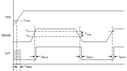
5.6 Timing Requirements
| PARAMETER | TEST CONDITION | MIN | TYP | MAX | UNIT | |
|---|---|---|---|---|---|---|
| tpd(HL) | High-to-low propagation delay(1) | VDD = 24 V, ±10-mV input overdrive, RL = 100 kΩ, VOH = 0.9 × VDD, VOL = 250 mV | 9.9 | µs | ||
| tpd(LH) | Low-to-high propagation delay(1) | VDD = 24 V, ±10-mV input overdrive, RL = 100 kΩ, VOH = 0.9 × VDD, VOL = 250 mV | 28.1 | µs | ||
| td(start)(2) | Startup delay | VDD = 5 V | 155 | µs | ||
| tr | Output rise time | VDD = 12 V, 10-mV input overdrive, RL = 100 kΩ, CL = 10 pF, VO = (0.1 to 0.9) × VDD | 2.7 | µs | ||
| tf | Output fall time | VDD = 12 V, 10-mV input overdrive, RL = 100 kΩ, CL = 10 pF, VO = (0.9 to 0.1) × VDD | 0.12 | µs | ||
(1) High-to-low and low-to-high refers to the transition at the input pin (SENSE).
(2) During power on, VDD must exceed 1.8 V for at least 150 µs (typ) before the output state reflects the input condition.
 Figure 5-1 Timing Diagram