ZHCSED3B November   2015  – December 2023 TPS3711

PRODUCTION DATA  

  1.   1
  2. 特性
  3. 应用
  4. 说明
  5. Pin Configuration and Functions
  6. Specifications
    1. 5.1 Absolute Maximum Ratings #GUID-795AD25B-5DDA-4725-83BA-87F5B93DF96A/ABSMAXNOTE
    2. 5.2 ESD Ratings
    3. 5.3 Recommended Operating Conditions
    4. 5.4 Thermal Information
    5. 5.5 Electrical Characteristics
    6. 5.6 Timing Requirements
    7. 5.7 Typical Characteristics
  7. Detailed Description
    1. 6.1 Overview
    2. 6.2 Functional Block Diagram
    3. 6.3 Feature Description
      1. 6.3.1 Input Pin (SENSE)
      2. 6.3.2 Output Pin (OUT)
    4. 6.4 Device Functional Modes
      1. 6.4.1 Normal Operation (VDD > UVLO)
      2. 6.4.2 Undervoltage Lockout (V(POR) < VDD < UVLO)
      3. 6.4.3 Power On Reset (VDD < V(POR))
  8. Application and Implementation
    1. 7.1 Application Information
      1. 7.1.1 Input and Output Configurations
      2. 7.1.2 Immunity to Input Pin Voltage Transients
    2. 7.2 Typical Application
      1. 7.2.1 Design Requirements
      2. 7.2.2 Detailed Design Procedure
        1. 7.2.2.1 Resistor Divider Selection
        2. 7.2.2.2 Pullup Resistor Selection
        3. 7.2.2.3 Input Supply Capacitor
      3. 7.2.3 Application Curves
    3. 7.3 Power Supply Recommendations
    4. 7.4 Layout
      1. 7.4.1 Layout Guidelines
      2. 7.4.2 Layout Example
  9. Device and Documentation Support
    1. 8.1 Documentation Support
      1. 8.1.1 Related Documentation
    2. 8.2 支持资源
    3. 8.3 Trademarks
    4. 8.4 静电放电警告
    5. 8.5 术语表
  10. Revision History
  11. 10Mechanical, Packaging, and Orderable Information

封装选项

机械数据 (封装 | 引脚)
散热焊盘机械数据 (封装 | 引脚)
订购信息

Pin Configuration and Functions

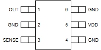
GUID-475AC123-192D-4D6B-9C07-B4C7E1FB26BF-low.gif Figure 4-1 DDC Package
6-Pin SOT
Top View
Table 4-1 Pin Functions
PIN I/O DESCRIPTION
NAME NO.
GND 2, 4, 6 Ground. Connect all three pins to ground.
OUT 1 O Comparator open-drain output. This pin is driven low when the voltage at this comparator is less than VIT–. The output goes high when the sense voltage rises above VIT+.
SENSE 3 I Comparator input. This pin is connected to the voltage to be monitored with the use of an external resistor divider. When the voltage at this pin drops below the threshold voltage VIT–, OUT is driven low.
VDD 5 I Supply-voltage input. Connect a 1.8-V to 36-V supply to VDD to power the device. It is good analog design practice to place a 0.1-µF ceramic capacitor close to this pin.