ZHCSL90 August 2020 TPS25980
PRODUCTION DATA
- 1 特性
- 2 应用
- 3 说明
- 4 Revision History
- 5 Device Comparison Table
- 6 Pin Configuration and Functions
- 7 Specifications
-
8 Detailed Description
- 8.1 Overview
- 8.2 Functional Block Diagram
- 8.3 Feature Description
- 8.4 Fault Response
- 8.5 Device Functional Modes
-
9 Application and Implementation
- 9.1 Application Information
- 9.2
Typical Application: Patient Monitoring System in Medical Applications
- 9.2.1 Design Requirements
- 9.2.2
Detailed Design Procedure
- 9.2.2.1 Device Selection
- 9.2.2.2 Setting the Current Limit Threshold: RILIM Selection
- 9.2.2.3 Setting the Undervoltage Lockout Set Point
- 9.2.2.4 Choosing the Current Monitoring Resistor: RIMON
- 9.2.2.5 Setting the Output Voltage Ramp Time (TdVdt)
- 9.2.2.6 Setting the Load Handshake (LDSTRT) Delay
- 9.2.2.7 Setting the Transient Overcurrent Blanking Interval (tITIMER)
- 9.2.2.8 Setting the Auto-Retry Delay and Number of Retries
- 9.2.3 Application Curves
- 9.3 System Examples
- 10Power Supply Recommendations
- 11Layout
- 12Device and Documentation Support
- 13Mechanical, Packaging, and Orderable Information
8.3.7 Load Detect/Handshake (LDSTRT)
The LDSTRT pin provides a mechanism for the downstream load circuit to indicate to the TPS25980x that the load is present and has powered up successfully. This allows the system to have additional control over the conditions in which power is presented to the load and disconnect the power when the load is not present or unable to provide a valid handshake signal after an expected boot-up time.
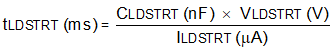
Once the TPS25980x completes the startup sequence and the output reaches the full voltage, it asserts the PG signal. At the same time, it also starts charging the capacitor on the LDSTRT pin (CLDSTRT) with an internal current source (ILDSTRT). If the LDSTRT pin voltage rises above VLDSTRT before the load circuit pulls it low, the TPS25980x detects the condition as a LDSTRT fault and turns off the FET to power down the load. The time to trigger the LDSTRT fault can be calculated from the following equation:
During normal operation, if at any time the load circuit releases the active pull-down on the LDSTRT pin, the capacitor CLDSTRT would start charging up again and eventually trigger a shutdown due to LDSTRT fault once the capacitor charges up to VLDSTRT.
Once the TPS25980x turns off due to LDSTRT fault, it can be turned ON again in 3 ways:
- LDSTRT pin is driven low
- Input supply voltage is driven low (< VUVP(F)) and then driven high (> VUVP(R))
- EN/UVLO voltage is driven low (< VSD) and then driven high (> VUVLO(R))
Tie the LDSTRT pin to ground if this functionality is not needed.
 Figure 8-6 Successful LDSTRT Handshake
 Figure 8-7 Unsuccessful LDSTRT Handshake
The LDSTRT pin can also be used to implement a load or module detect function wherein the output power is presented only when the load or module is plugged in. A typical use case for this function is on optical module power supply rails in Switches/Routers or similar networking end equipment. The LDSTRT pin should be tied to a corresponding pin on the module connector which gets pulled low by the module when it is plugged in. An example of such a signal is ModPrsL on QSFP-DD modules.
In this scheme, initially when the TPS25980x is powered up or enabled, the output charges up and PG is asserted. If the module is not plugged in, there is no external pull-down on the LDSTRT pin and the pin voltage starts rising due to internal pull-up . Once the LDSTRT pin voltage exceeds VLDSTRT, the TPS25980x turns off the output power. If the module is plugged in later, the LDSTRT pin is pulled low by the module and the TPS25980x turns on the output power.
 Figure 8-8 Optical Module Plug-In Detection Using LDSTRT