ZHCSJQ2A May 2019 – August 2019 TPS2596
PRODUCTION DATA.
- 1 特性
- 2 应用
- 3 说明
- 4 修订历史记录
- 5 器件比较表
- 6 Pin Configuration and Functions
- 7 Specifications
-
8 Detailed Description
- 8.1 Overview
- 8.2 Functional Block Diagram
- 8.3 Feature Description
- 8.4 Device Functional Modes
-
9 Application and Implementation
- 9.1 Application Information
- 9.2
Typical Application
- 9.2.1 Precision Current Limiting and Protection for White Goods
- 9.2.2 Design Requirements
- 9.2.3 Detailed Design Procedure
- 9.2.4 Support Component Selection: RFLT and CIN
- 9.2.5 Application Curves
- 9.3 System Examples
- 10Power Supply Recommendations
- 11Layout
- 12器件和文档支持
- 13机械、封装和可订购信息
7.8 Typical Characteristics
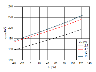
A.
Figure 2. TPS25963x Quiescent Current | OUT = OPEN |
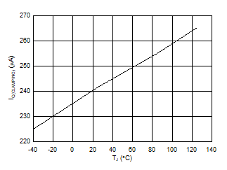
A.
Figure 4. TPS25962x Quiescent Current During Overvoltage Clamping | OVCSEL = OPEN, VIN = 19 V |
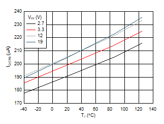
A.
Figure 3. TPS25962x Quiescent Current | OUT = OPEN |
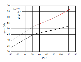
A.
Figure 5. Disabled State Current | VEN/UVLO = 1 V |
A.
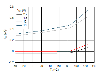
Figure 6. Shutdown Current | VEN/UVLO = 0 V |
A.
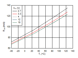
Figure 7. ON Resistance | IOUT = 200 mA |
A.
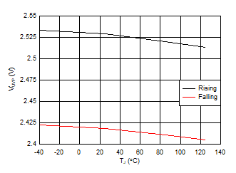
Figure 8. IN Supply Undervoltage Threshold 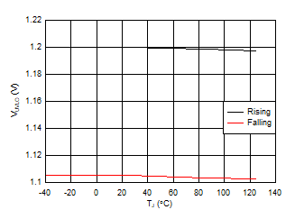
A.
Figure 9. EN/UVLO Disable Threshold | VIN = 12 V |
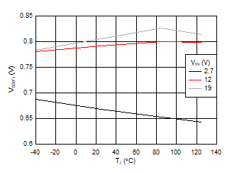
A.
Figure 10. EN/UVLO Shutdown Threshold for Lowest Current Consumption 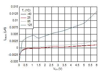
A.
Figure 11. EN/UVLO Pin Leakage Current 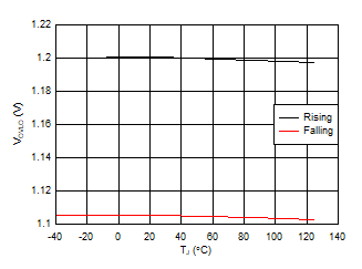
A.
Figure 12. TPS25963x Overvoltage Lockout Threshold 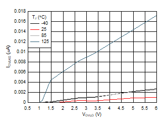
A.
Figure 13. TPS25963x OVLO Pin Leakage Current 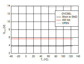
A.
Figure 14. TPS25962x Overvoltage Clamp Threshold | ROUT = 10 KΩ |
A.
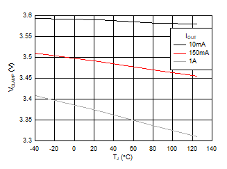
Figure 15. TPS25962x Overvoltage Clamping Voltage | OVCSEL = Short to GND, VIN = 4.2 V |
A.
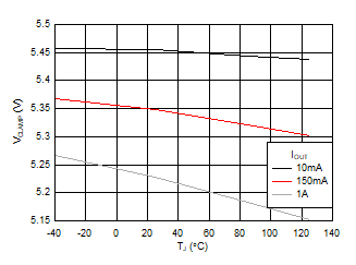
Figure 16. TPS25962x Overvoltage Clamping Voltage | OVCSEL = 400 KΩ to GND, VIN = 6.1 V |
A.
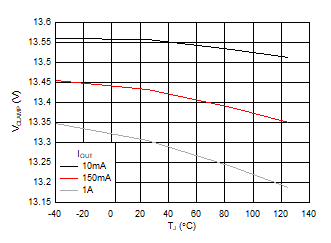
Figure 17. TPS25962x Overvoltage Clamping Voltage | OVCSEL = OPEN, VIN = 14.4 V |
A.
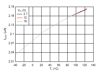
Figure 18. DVDT Charging Current 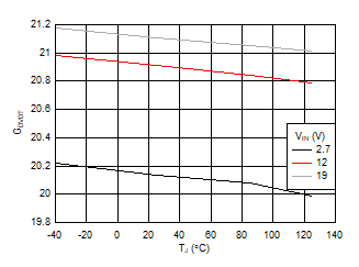
A.
Figure 19. DVDT Gain 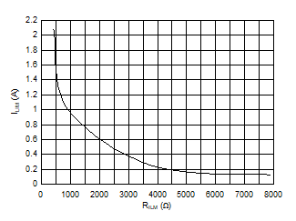
A.
Figure 20. Current Limit vs RILM 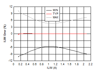
A.
Figure 21. Current Limit Accuracy | Across Process, Voltage and Temperature Corners, VDS = 0.5 V |
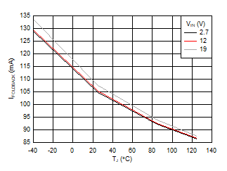
A.
Figure 22. Current Limit Foldback | VOUT = 0 V, RILM = 7.87 KΩ |
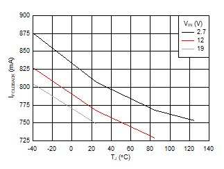
A.
Figure 23. Current Limit Foldback | VOUT = 0 V, RILM = 453 Ω |
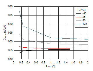
A.
Figure 24. Current Monitor Gain 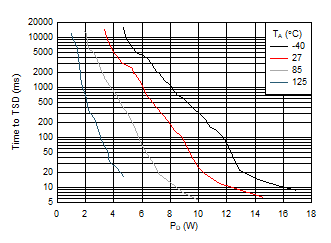
A.
Figure 26. Thermal Shutdown Plot | 1- Layer PCB: 2 oz Cu with GND Plane area: 4.43 cm2 (Top) |
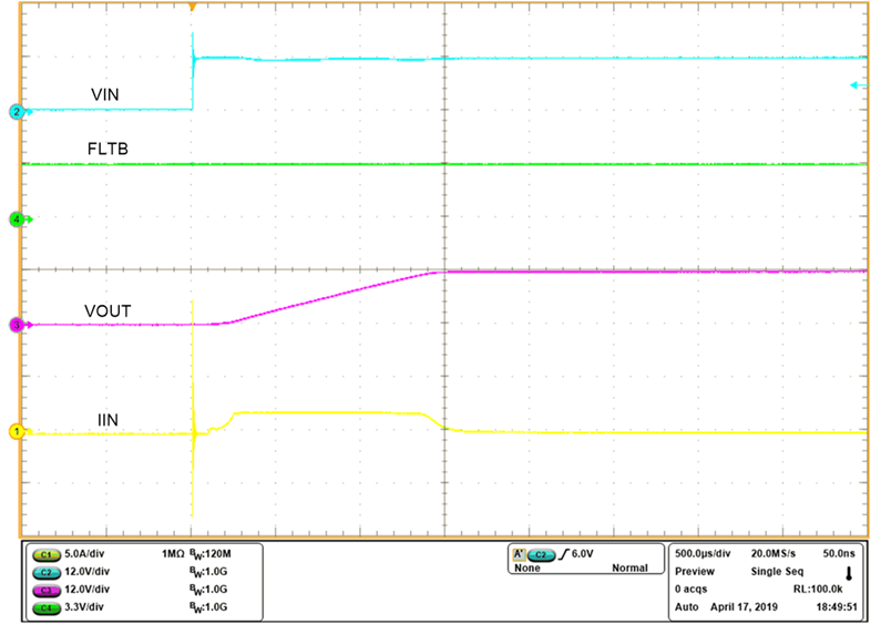
A.
Figure 28. Input Hotplug Response | VIN = 12 V, COUT = 220 μF, RILM = 453 Ω |
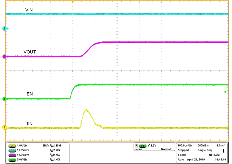
A.
Figure 30. Output Voltage Ramp and Inrush Current at Start Up, CdVdT = OPEN | VIN = 12 V, COUT = 10 μF, RILM = 453 Ω, CDVDT = OPEN |
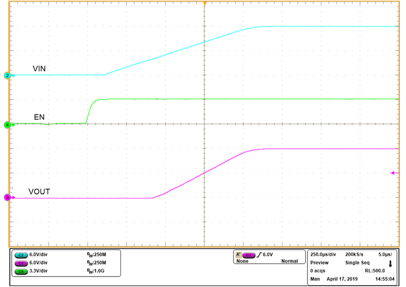
A.
Figure 32. Turn ON with VIN | VIN = 12 V, VEN = 3.3 V |
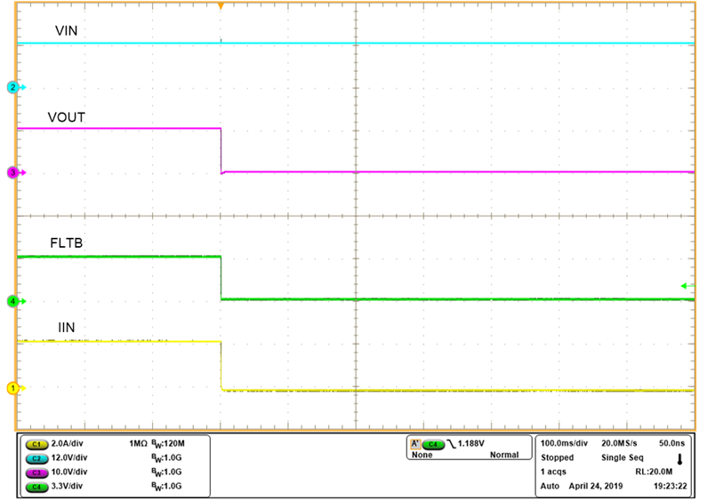
A.
Figure 34. Thermal Shutdown Latch-off Response - TPS2596x0 | VIN = 12 V, RILM = 453 Ω, ROUT = 5 Ω |
A.
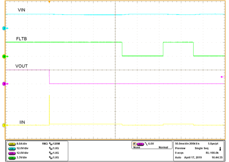
Figure 36. Short-Circuit While ON Response | VIN = 12 V, RILM = 453 Ω |
A.
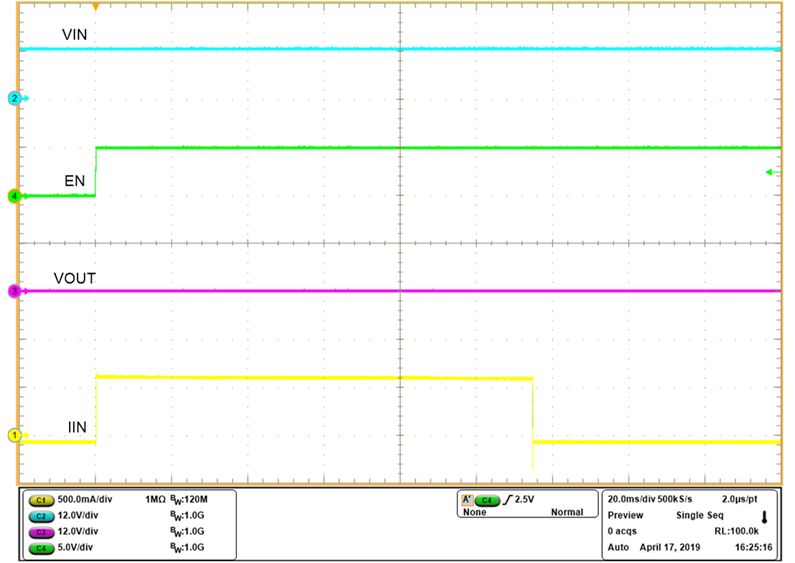
Figure 38. Power Up Into Short-Circuit | VIN = 12 V, RILM = 453 Ω |
A.
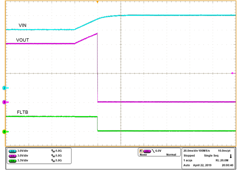
Figure 40. TPS25963x Overvoltage Lockout Response | VIN increased from 12 V to 15 V |
A.
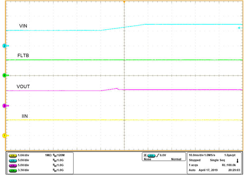
Figure 42. TPS25962x Overvoltage Clamp Response | OVCSEL = 400 KΩ to GND, VIN increased from 5 V to 7 V |
A.
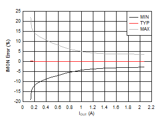
Figure 25. Current Monitor Accuracy | Across Process, Voltage and Temperature Corners, All values normalized to mean GIMON value of 656 μA/A |
A.
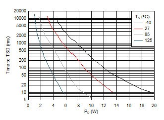
Figure 27. Thermal Shutdown Plot | 2- Layer PCB: 2 oz Cu with GND Plane area: 4.93 cm2 (Top) and 1.07 cm2 (Bottom) |
A.
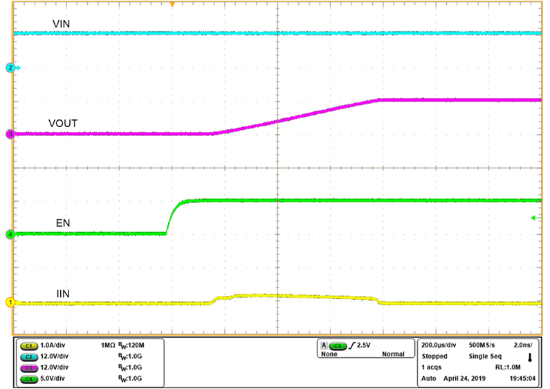
Figure 29. Output Voltage Ramp and Inrush Current at Start Up, CdVdT = 2200 pF | VIN = 12 V, COUT = 10 μF, RILM = 453 Ω, CDVDT = 2200 pF |
A.
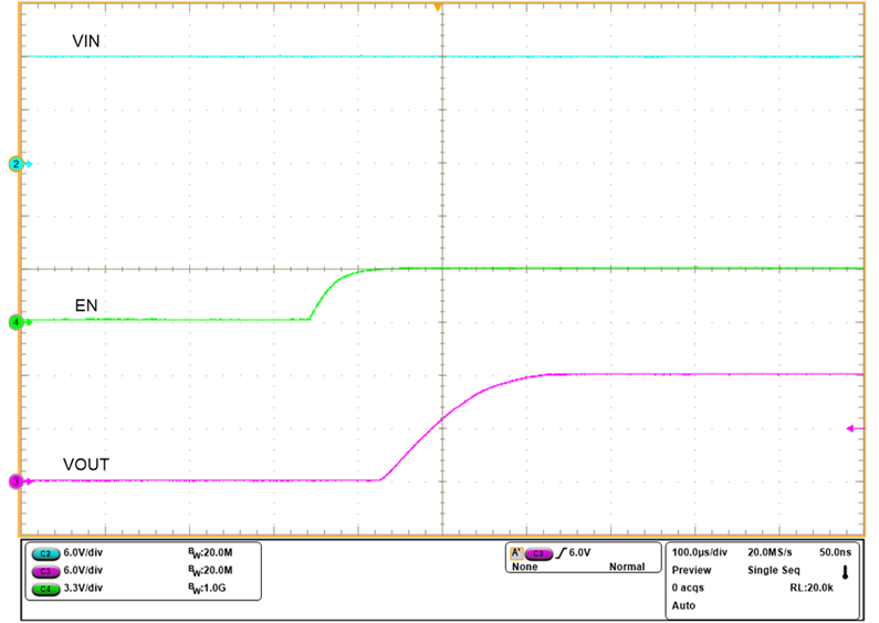
Figure 31. Turn ON with EN | VIN = 12 V, VEN = 3.3 V |
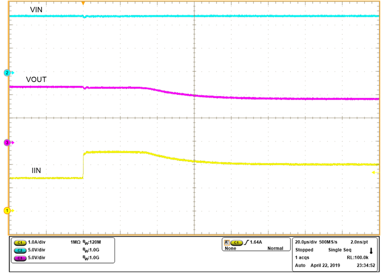
A.
Figure 33. Overcurrent Response | VIN = 12 V, RILM = 453 Ω, ROUT Varied From 8.33 Ω to 4.54 Ω |
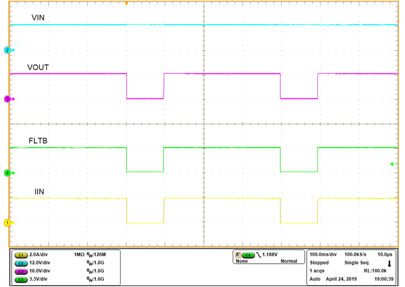
A.
Figure 35. Thermal Shutdown Auto-Retry Response - TPS2596x1 | VIN = 12 V, RILM = 453 Ω, ROUT = 5 Ω |
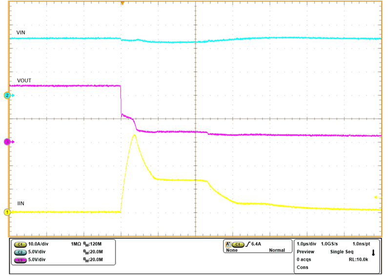
A.
Figure 37. Short-Circuit While ON Response (Zoomed In) | VIN = 12 V, RILM = 453 Ω |
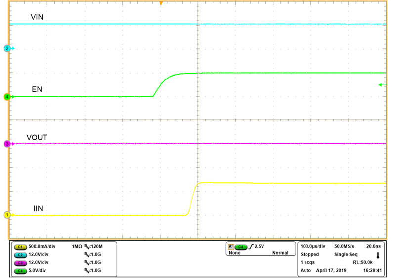
A.
Figure 39. Power Up Into Short-Circuit (Zoomed In) | VIN = 12 V, RILM = 453 Ω |
A.
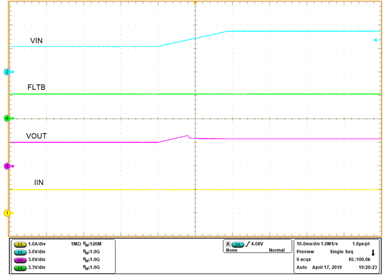
Figure 41. TPS25962x Overvoltage Clamp Response | OVCSEL = Shorted to GND, VIN increased from 3 V to 5 V |
A.
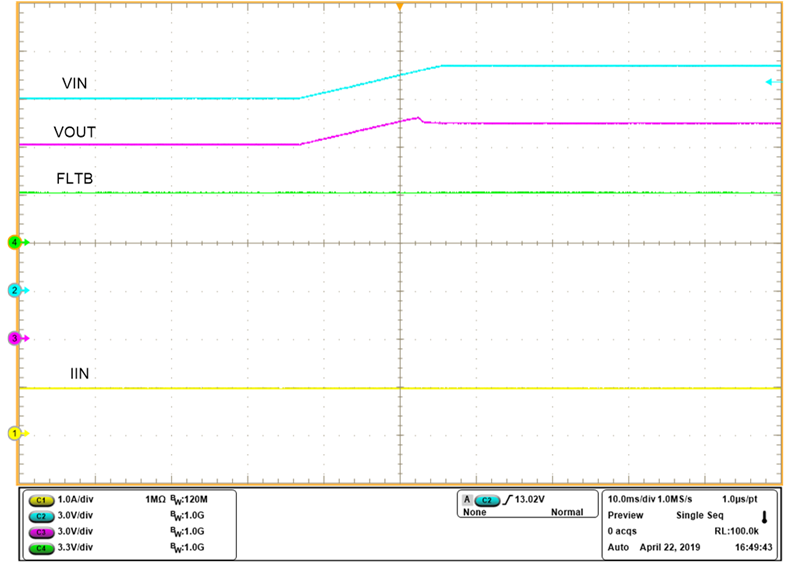
Figure 43. TPS25962x Overvoltage Clamp Response | OVCSEL = OPEN, VIN increased from 12 V to 14 V |