ZHCSL91B October 2020 – March 2022 TPS25947
PRODUCTION DATA
- 1 特性
- 2 应用
- 3 说明
- 4 Revision History
- 5 Device Comparison Table
- 6 Pin Configuration and Functions
- 7 Specifications
-
8 Detailed Description
- 8.1 Overview
- 8.2 Functional Block Diagram
- 8.3
Feature Description
- 8.3.1 Input Reverse Polarity Protection
- 8.3.2 Undervoltage Lockout (UVLO and UVP)
- 8.3.3 Overvoltage Lockout (OVLO)
- 8.3.4 Overvoltage Clamp (OVC)
- 8.3.5 Inrush Current, Overcurrent, and Short Circuit Protection
- 8.3.6 Analog Load Current Monitor
- 8.3.7 Reverse Current Protection
- 8.3.8 Overtemperature Protection (OTP)
- 8.3.9 Fault Response and Indication (FLT)
- 8.3.10 Auxiliary Channel Control (AUXOFF)
- 8.3.11 Power Good Indication (PG)
- 8.4 Device Functional Modes
- 9 Application and Implementation
- 10Power Supply Recommendations
- 11Layout
- 12Device and Documentation Support
- 13Mechanical, Packaging, and Orderable Information
9.5 Priority Power MUXing
Applications having two energy sources such as PCIe cards, Tablets and Portable battery powered equipment require preference of one source to another. For example, mains power (wall-adapter) has the priority over the internal battery back-up power. These applications demand for switchover from mains power to backup power only when main input voltage falls below a user defined threshold. The TPS25947xx devices provide a simple solution for priority power multiplexing needs.
Figure 9-10 below shows a typical priority power multiplexing implementation using TPS259470x devices. When primary (priority) power source (IN1) is present and within the valid range (not in UV/OV condition), the primary path device path powers the OUT bus irrespective of whether auxiliary supply voltage (VIN2) is greater than, equal to or less than primary supply voltage (VIN1). The device in auxiliary path is held in off condition by forcing its OVLO pin to high using the AUXOFF signal from the primary path device.
After the primary supply voltage falls outside the user-defined valid operating range (UV/OV condition), the primary path device de-asserts the AUXOFF which signals the auxiliary path device to turn on and the system starts operating from the auxiliary supply. During this transition, the auxiliary path device bypasses its dVdt limited startup and performs a fast recovery to start delivering power within tSWOV.
When the primary supply is restored, the primary path device turns on fully at a defined slew rate and then asserts its AUXOFF pin high to turn the auxiliary path device off, allowing a seamless transition from auxiliary to the primary supply with minimal output voltage droop and with no shoot-through current.
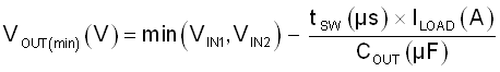
A key consideration in power MUXing applications is the minimum voltage the output bus droops to during the switchover from one supply to another. This in turn depends on multiple factors including the output load current (ILOAD), output bus hold-up capacitance (COUT) and switchover time (tSW).
While switching from primary supply (VIN1) to auxiliary supply (VIN2), the minimum bus voltage can be calculated using Equation 19. Here, the switchover time (tSW) is equal to the fast OVLO recovery time (tSWOV) taken by the TPS259470x variants to turn on fully and start delivering current to the load.
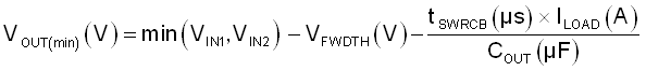
While switching from auxiliary supply (VIN2) to primary supply (VIN1), the minimum bus voltage can be calculated using Equation 20. Here the maximum switchover time is equal to the RCB recovery time (tSWRCB), depending on whether VIN1 is equal to or lower than VIN2 to start with.
The AUXOFF pins of the devices can be used as a digital indication to identify which of the 2 supplies is active and delivering power to the load.
 Figure 9-10 Priority Power MUXing with 2 ×
TPS259470x - Option 1
Figure 9-10 Priority Power MUXing with 2 ×
TPS259470x - Option 1This configuration provides the most compact priority power MUXing solution with multiple benefits, including active current limit protection on both channels as well as overvoltage protection on primary channel. It also provides the fastest switchover time from primary to auxiliary, but at the cost of a slightly increased quiescent current on the auxiliary path while primary path is active. Also, it uses the fewest external components, but at the cost of bypassing overvoltage protection on auxiliary channel.
The following waveforms illustrate the TPS259470x performance in a priority power MUXing configuration.
 Figure 9-11 TPS259470x Power MUX - Switchover from
Primary to Auxiliary Supply
Figure 9-11 TPS259470x Power MUX - Switchover from
Primary to Auxiliary Supply Figure 9-12 TPS259470x Power MUX - Switchover from
Auxiliary to Primary Supply
Figure 9-12 TPS259470x Power MUX - Switchover from
Auxiliary to Primary SupplyThere's a possible variation to the above configuration in case overvoltage protection is needed on both channels. This needs an additional signal N-FET to drive the OVLO pin of the auxiliary path device as shown in Figure 9-13 below. The switchover times are similar to the previous configuration.
 Figure 9-13 Priority Power MUXing with 2 ×
TPS259470x - Option 2
Figure 9-13 Priority Power MUXing with 2 ×
TPS259470x - Option 2Another variation of the previous configuration ensures minimum quiescent current on the auxiliary chanel while primary channel is active, but at the cost of additional N-FET to drive the EN/UVLO pin of auxiliary path device as shown in Figure 9-14 below. At the same time, it has a higher switchover delay from primary to auxiliary supply as compared to the previous configuration.
 Figure 9-14 Priority Power MUXing with 2 ×
TPS259470x - Option 3
Figure 9-14 Priority Power MUXing with 2 ×
TPS259470x - Option 3While switching from a higher supply rail to lower supply rail, the minimum bus voltage can be calculated using Equation 21. Here, the switchover time is equal to the time taken by the device to come out of reverse current blocking state (tSWRCB).
While switching from a lower supply rail to higher supply rail, the minimum bus voltage can be calculated using Equation 22. Here, the switchover time (tSW) is the time taken by the device to turn on fully and start delivering current to the load, which is equal to the device turn-on time (tON), which in turn includes the turn-on delay (tD,ON) and rise time (tR) determined by the dVdt capacitor (CdVdt) and bus voltage.
All the preceding configurations provide a priority power MUXing solution with active current limit protection response. In case circuit breaker response is prefered, it is possible to implement a solution using TPS259474x devices as shown in Figure 9-15 below. Here, the EN/UVLO signal of the primary path device is used to control the OVLO of the auxiliary path device. This ensures that auxiliary path device is turned on only when the primary supply falls below a user-defined undervoltage (UVLO) threshold. In this configuration, supply overvoltage protection is not available on both channels. The PG pins of the devices can be used as a digital indication to identify which of the 2 supplies is active and delivering power to the load.
 Figure 9-15 Priority power MUXing with 2 ×
TPS259474x
Figure 9-15 Priority power MUXing with 2 ×
TPS259474xWhile switching from one supply rail to the other, the minimum bus voltage can be calculated using Equation 23. Here, the maximum switchover time (tSW) is the time taken by the device to turn on and start delivering power to the load, which is equal to the device turn-on time (tON), which in turn includes the turn-on delay (tD,ON) and rise time (tR) determined by the dVdt capacitor (CdVdt) and bus voltage.
- The TPS259472x (OVC variants) are not recommended for use in power MUXing or ORing applications. While the device is in clamping state, if the output is forced to a higher voltage by the other channel, the device can get damaged.
- Power MUXing can be done either between two similar rails (such as 12-V Primary and 12-V Aux, 3.3-V Primary and 3.3-V Aux) or between dissimilar rails (such as 12-V Primary and 5-V Aux or vice versa).
- For power MUXing cases with skewed voltage combinations, care must be taken to design circuit components on PGTH/EN/OVLO pins for the lower voltage channel devices such that the Absolute maximum ratings on those pins are not exceeded when higher voltage is present on the other channel. Also, the dVdt pin capacitor rating must be chosen based on the highest of the 2 supplies. Refer to Recommended Operating Conditions table for more details.