ZHCSMV6A October 2021 – December 2021 TPS22998
PRODUCTION DATA
- 1 特性
- 2 应用
- 3 说明
- 4 Revision History
- 5 Pin Configuration and Functions
-
6 Specifications
- 6.1 Absolute Maximum Ratings
- 6.2 ESD Ratings
- 6.3 Recommended Operating Conditions
- 6.4 Thermal Information
- 6.5 Electrical Characteristics (VBIAS = 5 V)
- 6.6 Electrical Characteristics (VBIAS = 3.3 V)
- 6.7 Electrical Characteristics (VBIAS = 2.2 V)
- 6.8 Switching Characteristics (VBIAS = 2.2 V to 5 V)
- 6.9 Timing Diagram
- 6.10 Typical Characteristics
- 7 Detailed Description
- 8 Application and Implementation
- 9 Power Supply Recommendations
- 10Layout
- 11Device and Documentation Support
- 12Mechanical, Packaging, and Orderable Information
5 Pin Configuration and Functions
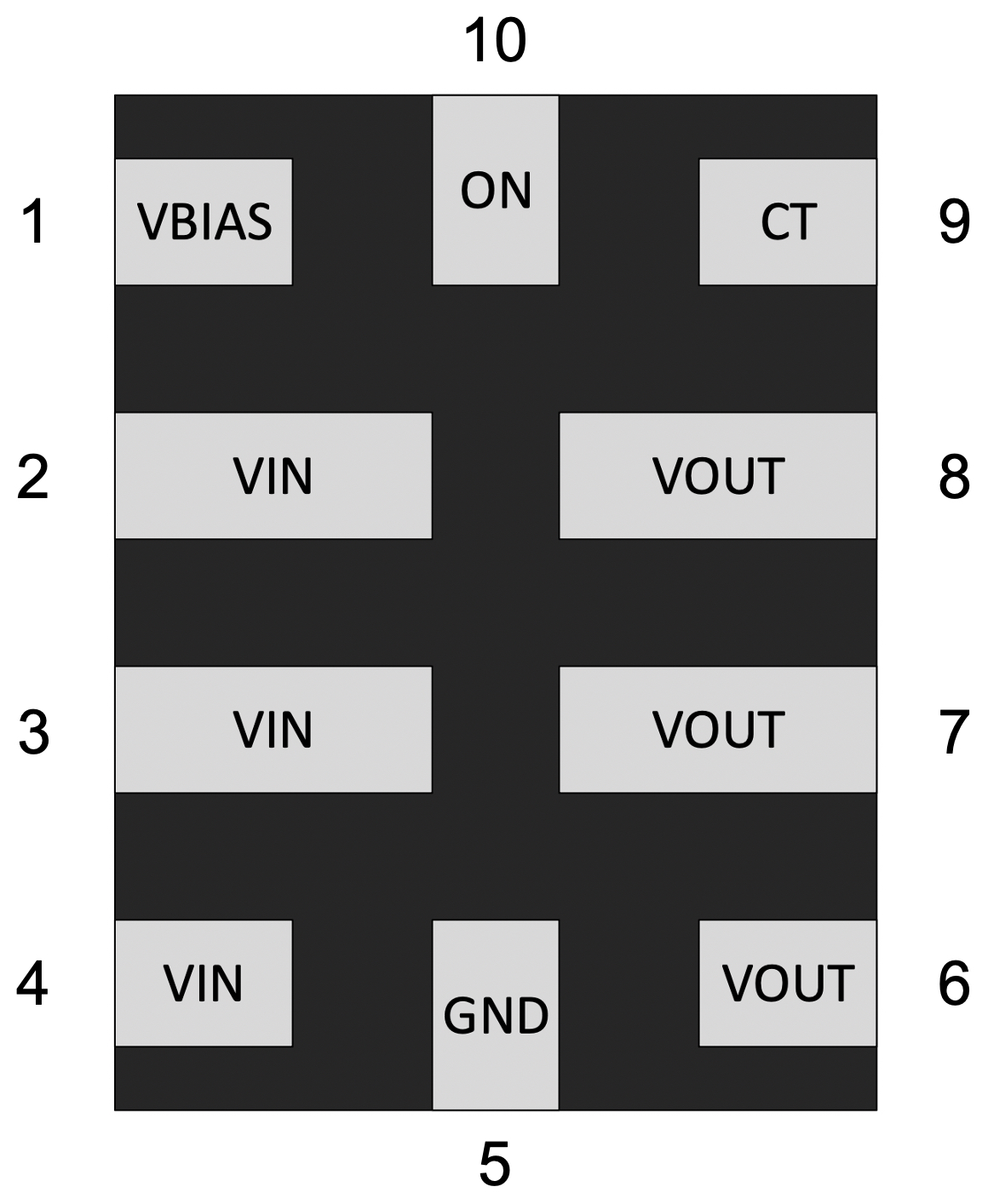
 Figure 5-1 TPS22998 RYZ Package, 10-Pin WQFN (Top View)
Table 5-1 Pin Functions
| PIN | I/O(1) | DESCRIPTION | |
|---|---|---|---|
| NAME | NO. | ||
VBIAS | 1 | I | Device bias supply |
VIN | 2, 3, 4 | I | Switch input |
GND | 5 | G | Device ground |
VOUT | 6, 7, 8 | O | Switch output |
CT | 9 | I | Slew rate control – can be pulled up, left floating, or tie to ground |
ON | 10 | I | Enable pin |
(1) I = Input, O = Output, I/O = Input or Output, G = Ground, P = Power.