ZHCSHY9 April   2018 TPS22810-Q1

PRODUCTION DATA.  

  1. 特性
  2. 应用
  3. 说明
    1.     简化原理图
  4. 修订历史记录
  5. Pin Configuration and Functions
    1.     Pin Functions
  6. Specifications
    1. 6.1 Absolute Maximum Ratings
    2. 6.2 ESD Ratings
    3. 6.3 Recommended Operating Conditions
    4. 6.4 Thermal Information
    5. 6.5 Electrical Characteristics
    6. 6.6 Switching Characteristics
    7. 6.7 Typical DC Characteristics
    8. 6.8 Typical AC Characteristics
  7. Parameter Measurement Information
  8. Detailed Description
    1. 8.1 Overview
    2. 8.2 Functional Block Diagram
    3. 8.3 Feature Description
      1. 8.3.1 On and Off Control
      2. 8.3.2 Quick Output Discharge (QOD)
        1. 8.3.2.1 QOD when System Power is Removed
        2. 8.3.2.2 Internal QOD Considerations
      3. 8.3.3 EN/UVLO
      4. 8.3.4 Adjustable Rise Time (CT)
      5. 8.3.5 Thermal Shutdown
    4. 8.4 Device Functional Modes
  9. Application and Implementation
    1. 9.1 Application Information
      1. 9.1.1 ON and OFF Control
      2. 9.1.2 Input Capacitor (Optional)
      3. 9.1.3 Output Capacitor (Optional)
    2. 9.2 Typical Application
      1. 9.2.1 Design Requirements
      2. 9.2.2 Detailed Design Procedure
        1. 9.2.2.1 Shutdown Sequencing During Unexpected Power Loss
        2. 9.2.2.2 VIN to VOUT Voltage Drop
        3. 9.2.2.3 Inrush Current
      3. 9.2.3 Application Curves
  10. 10Power Supply Recommendations
  11. 11Layout
    1. 11.1 Layout Guidelines
    2. 11.2 Layout Example
    3. 11.3 Thermal Considerations
  12. 12器件和文档支持
    1. 12.1 器件支持
      1. 12.1.1 开发支持
    2. 12.2 文档支持
      1. 12.2.1 相关文档
    3. 12.3 接收文档更新通知
    4. 12.4 社区资源
    5. 12.5 商标
    6. 12.6 静电放电警告
    7. 12.7 Glossary
  13. 13机械、封装和可订购信息

封装选项

机械数据 (封装 | 引脚)
散热焊盘机械数据 (封装 | 引脚)
订购信息

Pin Configuration and Functions

DBV Package
6-Pin SOT-23
Top View
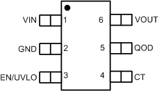
TPS22810-Q1 DevicePinOutTopView_SLVSDH0.gif

Pin Functions

PIN I/O DESCRIPTION
NAME NO.
CT 4 O Switch slew rate control. Can be left floating
EN/UVLO 3 I Active high switch control input and UVLO adjustment. Do not leave floating
GND 2 Device ground
QOD 5 O Quick Output Discharge pin. This functionality can be enabled in one of three ways:
  • Placing an external resistor between VOUT and QOD
  • Tying QOD directly to VOUT and using the internal resistor value (RPD)
  • Disabling QOD by leaving pin floating
See the Quick Output Discharge (QOD) for more information
VIN 1 I Switch input. Place ceramic bypass capacitor(s) between this pin and GND
VOUT 6 O Switch output