ZHCSIQ0F August   2018  – August 2020 TPS2120 , TPS2121

PRODUCTION DATA  

  1. 特性
  2. 应用
  3. 说明
  4. Revision History
  5. Device Comparison Table
  6. Pin Configuration and Functions
    1.     7
  7. Specifications
    1. 7.1 Absolute Maximum Ratings
    2. 7.2 ESD Ratings
    3. 7.3 Recommended Operating Conditions
    4. 7.4 Thermal Information
    5. 7.5 Electrical Characteristics
    6. 7.6 Typical Characteristics
  8. Parameter Measurement Information
  9. Detailed Description
    1. 9.1 Overview
    2. 9.2 Functional Block Diagram
    3. 9.3 Feature Description
      1. 9.3.1 Input Settling Time and Output Soft Start Control (SS)
        1. 9.3.1.1 Slew Rate vs. CSS Capacitor
      2. 9.3.2 Active Current Limiting (ILM)
      3. 9.3.3 Short-Circuit Protection
      4. 9.3.4 Thermal Protection (TSD)
      5. 9.3.5 Overvoltage Protection (OVx)
      6. 9.3.6 Fast Reverse Current Blocking (RCB)
      7. 9.3.7 Output Voltage Dip and Fast Switchover Control (TPS2121 only)
      8. 9.3.8 Input Voltage Comparator (VCOMP)
    4. 9.4 TPS2120 Device Functional Modes
    5. 9.5 TPS2121 Device Functional Modes
  10. 10Application and Implementation
    1. 10.1 Application Information
    2. 10.2 Typical Application
      1. 10.2.1 Manual Switchover Schematic
      2. 10.2.2 Design Requirements
      3. 10.2.3 Detailed Design Description
      4. 10.2.4 Design Procedure
        1. 10.2.4.1 Selecting PR1 and CP2 Resistors
        2. 10.2.4.2 Selecting OVx Resistors
        3. 10.2.4.3 Selecting Soft-Start Capacitor and Current Limit Resistors
      5. 10.2.5 Application Curves
    3. 10.3 Automatic Switchover with Priority (XCOMP)
      1. 10.3.1 Application Schematic
      2. 10.3.2 Design Requirements
      3. 10.3.3 Detailed Design Description
      4. 10.3.4 Design Procedure
        1. 10.3.4.1 Selecting PR1 and CP2 Resistors
      5. 10.3.5 Application Curves
    4. 10.4 Automatic Seamless Switchover with Priority (XREF)
      1. 10.4.1 Application Schematic
      2. 10.4.2 Design Requirements
      3. 10.4.3 Detailed Design Description
      4. 10.4.4 Application Curves
    5. 10.5 Highest Voltage Operation (VCOMP)
      1. 10.5.1 Application Schematic
      2. 10.5.2 Design Requirements
      3. 10.5.3 Detailed Design Description
      4. 10.5.4 Detailed Design Procedure
      5. 10.5.5 Application Curves
    6. 10.6 Reverse Polarity Protection with TPS212x
    7. 10.7 Hotplugging with TPS212x
  11. 11Power Supply Recommendations
  12. 12Layout
    1. 12.1 Layout Guidelines
    2. 12.2 Layout Example
  13. 13Device and Documentation Support
    1. 13.1 Documentation Support
      1. 13.1.1 Related Links
    2. 13.2 接收文档更新通知
    3. 13.3 支持资源
    4. 13.4 Trademarks
    5. 13.5 静电放电警告
    6. 13.6 术语表
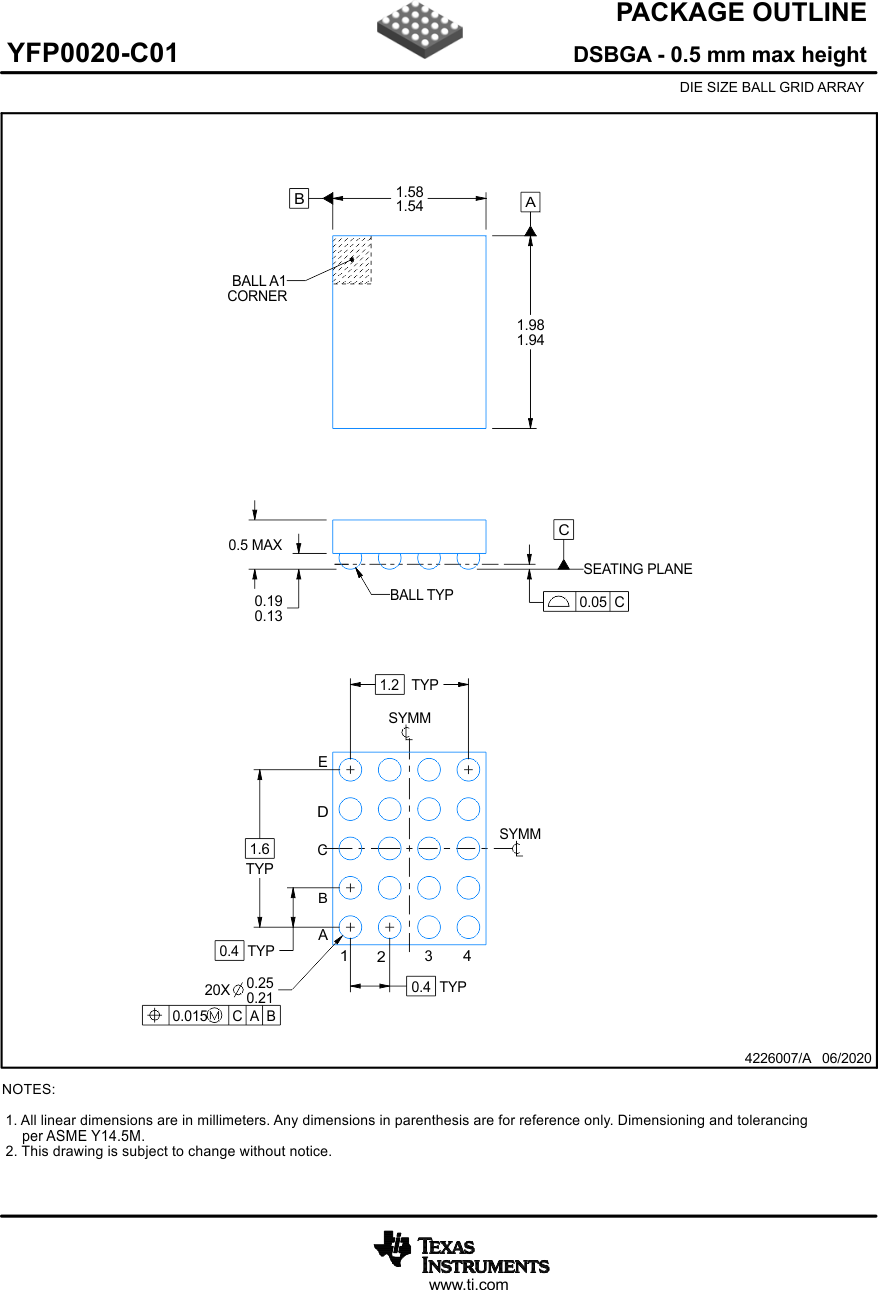
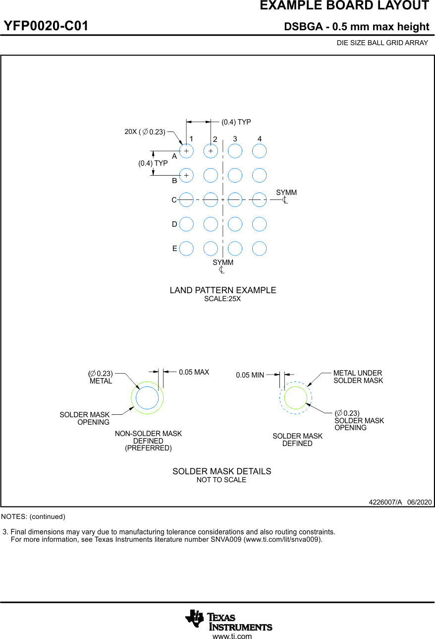
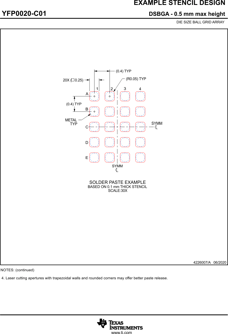
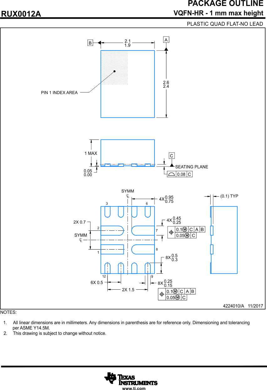
  14. 14Mechanical, Packaging, and Orderable Information

封装选项

请参考 PDF 数据表获取器件具体的封装图。

机械数据 (封装 | 引脚)
  • YFP|20
散热焊盘机械数据 (封装 | 引脚)
订购信息

Mechanical, Packaging, and Orderable Information

The following pages include mechanical, packaging, and orderable information. This information is the most current data available for the designated devices. This data is subject to change without notice and revision of this document. For browser-based versions of this data sheet, refer to the left-hand navigation.

GUID-20200709-SS0I-GP1K-WM6B-WBF1LCPNKPLV-low.gif
GUID-20200709-SS0I-VVXJ-G9QR-320KVNPB8K0S-low.gif
GUID-20200709-SS0I-VF7F-3X5H-7ZKMV1H7RZL4-low.gif
GUID-20200819-CA0I-QMCW-68DJ-ZFMPRPNXWGCK-low.gif
GUID-20200819-CA0I-SWLC-2KBR-P6DB2DMWVHPN-low.gif
GUID-20200819-CA0I-BL2S-XGMX-BKPB70K0ZHNH-low.gif