ZHCSIQ0F August 2018 – August 2020 TPS2120 , TPS2121
PRODUCTION DATA
- 1 特性
- 2 应用
- 3 说明
- 4 Revision History
- 5 Device Comparison Table
- 6 Pin Configuration and Functions
- 7 Specifications
- 8 Parameter Measurement Information
-
9 Detailed Description
- 9.1 Overview
- 9.2 Functional Block Diagram
- 9.3
Feature Description
- 9.3.1 Input Settling Time and Output Soft Start Control (SS)
- 9.3.2 Active Current Limiting (ILM)
- 9.3.3 Short-Circuit Protection
- 9.3.4 Thermal Protection (TSD)
- 9.3.5 Overvoltage Protection (OVx)
- 9.3.6 Fast Reverse Current Blocking (RCB)
- 9.3.7 Output Voltage Dip and Fast Switchover Control (TPS2121 only)
- 9.3.8 Input Voltage Comparator (VCOMP)
- 9.4 TPS2120 Device Functional Modes
- 9.5 TPS2121 Device Functional Modes
- 10Application and Implementation
- 11Power Supply Recommendations
- 12Layout
- 13Device and Documentation Support
- 14Mechanical, Packaging, and Orderable Information
10.2.4.1 Selecting PR1 and CP2 Resistors
The TPS2120 does not contain a CP2 pin. Instead, a select pin (SEL), enables override of the PR1 / VREF comparison. Once the voltage on SEL is greater than VREF, the device will select IN2 as the output. For manual switchover, an external signal can be connected to the SEL pin. For this example, the external MCU signal is a 3.3-V enable.
The TPS2121 can be configured for manual switchover in a similar manner as the TPS2120. Instead of a SEL pin, the 3.3-V external MCU signal can be connected to CP2. As long as the voltage on CP2 is higher than PR1, the device will select IN2 as the output. When the voltage on CP2 drops below PR1, the device will switch back to IN1. Therefore, the resistor divider on PR1 is configured the same as above, with the 5 kΩ and 10.2 kΩ.
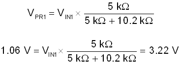
For additional precautions, the voltage on PR1 can also be configured. If the voltage on IN1 were to drop, the device can automatically switchover to IN2. In this example, if voltage on IN1 drops below IN2 (3.3 V) then the device will switch to IN2. Therefore, the resistor divider on PR1 should be configured such that the voltage on PR1 will drop below VREF, when IN1 dips below 3.3 V. The bottom resistor is chosen to be 5 kΩ due to it's commonality and minimal current leakage. If a smaller leakage is desired, a larger resistor can be used. With this configuration, the top resistor was selected to be 10.2 kΩ. With this resistor configuration, the device will switch to IN2 when the voltage on IN1 dips to 3.22 V. Refer to Table 9-2 for additional information regarding the switchover configuration.
See Equation 5 for the VPR1 Calculation