ZHCSIQ0F August 2018 – August 2020 TPS2120 , TPS2121
PRODUCTION DATA
- 1 特性
- 2 应用
- 3 说明
- 4 Revision History
- 5 Device Comparison Table
- 6 Pin Configuration and Functions
- 7 Specifications
- 8 Parameter Measurement Information
-
9 Detailed Description
- 9.1 Overview
- 9.2 Functional Block Diagram
- 9.3
Feature Description
- 9.3.1 Input Settling Time and Output Soft Start Control (SS)
- 9.3.2 Active Current Limiting (ILM)
- 9.3.3 Short-Circuit Protection
- 9.3.4 Thermal Protection (TSD)
- 9.3.5 Overvoltage Protection (OVx)
- 9.3.6 Fast Reverse Current Blocking (RCB)
- 9.3.7 Output Voltage Dip and Fast Switchover Control (TPS2121 only)
- 9.3.8 Input Voltage Comparator (VCOMP)
- 9.4 TPS2120 Device Functional Modes
- 9.5 TPS2121 Device Functional Modes
- 10Application and Implementation
- 11Power Supply Recommendations
- 12Layout
- 13Device and Documentation Support
- 14Mechanical, Packaging, and Orderable Information
9.3.7 Output Voltage Dip and Fast Switchover Control (TPS2121 only)
After input settling and soft start time, the TPS2121 utilizes a fast switchover to minimize output voltage drop. Where VSW is the output voltage when the switchover is triggered and tSW is the time until the output voltage stops dipping. The amount of voltage dip during the switchover time is a function of output load current (IOUT) and load capacitance (COUT). The minimum output voltage during switchover can be found using the following equations:
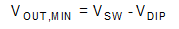
Where:
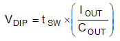
 Figure 9-7 Minimum Output Voltage During Fast Switchover
If switching from a lower to a higher voltage, the selected channel will not detect reverse voltage and shall turn on immediately using the current monitor to limit the output current to a safe level. If the output current reaches the current limit during fast switchover, this will increase the total time until the output reaches steady state.
 Figure 9-8 Fast Switchover from Lower to Higher Voltage
If an input is selected while the output voltage is still a higher voltage, that channel will continue to block reverse current by waiting to fast turn on until the output drops below the VRCB threshold.
 Figure 9-9 Fast Switchover from Higher to Lower Voltage