ZHCSLK6A July 2021 – December 2021 TPS1HC100-Q1
PRODUCTION DATA
- 1 特性
- 2 应用
- 3 说明
- 4 Revision History
- 5 Pin Configuration and Functions
- 6 Specifications
- 7 Parameter Measurement Information
-
8 Detailed Description
- 8.1 Overview
- 8.2 Functional Block Diagram
- 8.3
Feature Description
- 8.3.1 Accurate Current Sense
- 8.3.2 Programmable Current Limit
- 8.3.3 Inductive-Load Switching-Off Clamp
- 8.3.4
Full Protections and Diagnostics
- 8.3.4.1 Short-Circuit and Overload Protection
- 8.3.4.2 Open-Load and Short-to-Battery Detection
- 8.3.4.3 Short-to-Battery Detection
- 8.3.4.4 Reverse-Polarity and Battery Protection
- 8.3.4.5 Latch-Off Mode
- 8.3.4.6 Thermal Protection Behavior
- 8.3.4.7 UVLO Protection
- 8.3.4.8 Loss of GND Protection
- 8.3.4.9 Loss of Power Supply Protection
- 8.3.4.10 Reverse Current Protection
- 8.3.4.11 Protection for MCU I/Os
- 8.3.5 Diagnostic Enable Function
- 8.4 Device Functional Modes
- 9 Application and Implementation
- 10Power Supply Recommendations
- 11Layout
- 12Device and Documentation Support
- 13Mechanical, Packaging, and Orderable Information
9.2.3 Application Curves
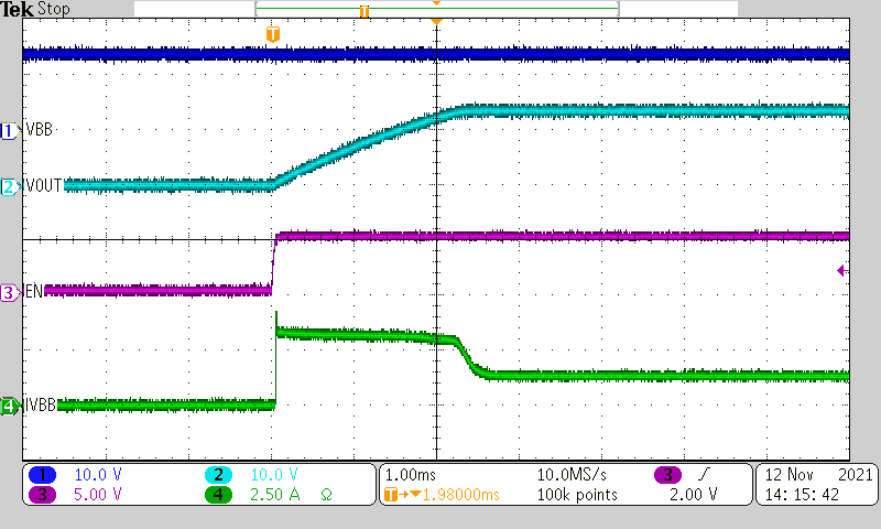
Figure 9-5 shows a test example of charging a 470-μF capacitor. Test conditions: VBB = 13.5 V, input is from low to high, load is a 470-µF capacitive load, ILIM pin is shorted to GND. CH4 is the output current. CH3 is the input step. CH2 is the output voltage, VOUT. CH1 is the supply voltage, VBB
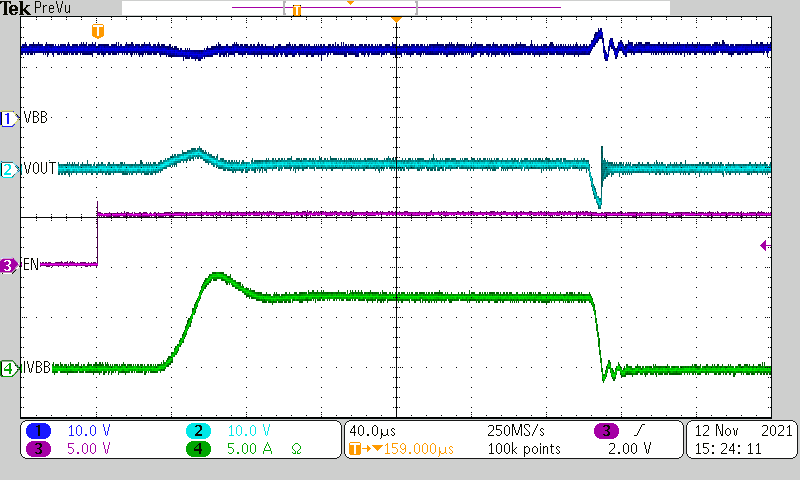
Figure 9-6 shows a test example of a enable into short-circuit inrush current limit. Test conditions: VBB= 13.5 V, input is low to high, load is 5 µH + 100 mΩ, ILIM pin is shorted to GND. CH4 is the output current. CH3 is the input step. CH2 is the output voltage, VOUT. CH1 is the supply voltage, VBB
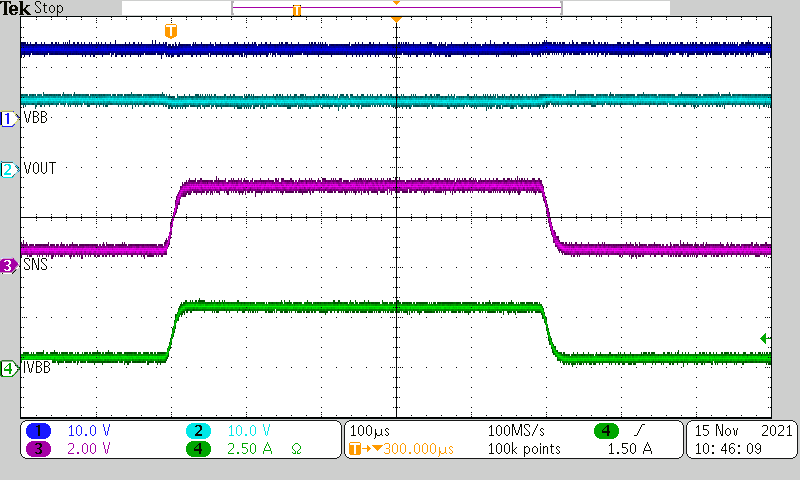
Figure 9-7 shows a test example of a load step from 500 mA to 3 A back to 500 mA. Test conditions: VBB= 13.5 V, input is high, load is 6.75 Ω and then changed to 4.5 Ω then back to 6.75 Ω, ILIM pin is shorted to GND. CH4 is the output current. CH3 is the SNS pin. CH2 is the output voltage, VOUT. CH1 is the supply voltage, VBB
 Figure 9-5 Charging a 470-μF Capacitor
 Figure 9-7 Load
Step
 Figure 9-6 Enable into Short Circuit