ZHCSLK6A July 2021 – December 2021 TPS1HC100-Q1
PRODUCTION DATA
- 1 特性
- 2 应用
- 3 说明
- 4 Revision History
- 5 Pin Configuration and Functions
- 6 Specifications
- 7 Parameter Measurement Information
-
8 Detailed Description
- 8.1 Overview
- 8.2 Functional Block Diagram
- 8.3
Feature Description
- 8.3.1 Accurate Current Sense
- 8.3.2 Programmable Current Limit
- 8.3.3 Inductive-Load Switching-Off Clamp
- 8.3.4
Full Protections and Diagnostics
- 8.3.4.1 Short-Circuit and Overload Protection
- 8.3.4.2 Open-Load and Short-to-Battery Detection
- 8.3.4.3 Short-to-Battery Detection
- 8.3.4.4 Reverse-Polarity and Battery Protection
- 8.3.4.5 Latch-Off Mode
- 8.3.4.6 Thermal Protection Behavior
- 8.3.4.7 UVLO Protection
- 8.3.4.8 Loss of GND Protection
- 8.3.4.9 Loss of Power Supply Protection
- 8.3.4.10 Reverse Current Protection
- 8.3.4.11 Protection for MCU I/Os
- 8.3.5 Diagnostic Enable Function
- 8.4 Device Functional Modes
- 9 Application and Implementation
- 10Power Supply Recommendations
- 11Layout
- 12Device and Documentation Support
- 13Mechanical, Packaging, and Orderable Information
8.3.4.10 Reverse Current Protection
Method 1: block diode connected with VBB. Both the device and load are protected when in reverse polarity. The blocking diode does not allow any of the current to flow during reverse battery condition.
Method 2 (GND network protection): only the high-side device is protected under this connection. The load reverse current is limited by the impedance of the load itself. Note when reverse polarity happens, the continuous reverse current through the power FET must not make the heat build up be greater than the absolute maximum junction temperature. This can be calculated using the RON(REV) value and the RθJA specification. In the reverse battery condition it is important that the FET comes on to lower the power dissipation. This action is achieved through the path from EN to system ground where the positive voltage is being applied. No matter what types of connection are between the device GND and the board GND, if a GND voltage shift happens, ensure the following proper connections for the normal operation:
- Connect the current limit programmable resistor to the device GND.
- Recommendation – resistor and
diode in parallel: a peak negative spike can occur when the inductive
load is switching off, which can damage the HSD or the diode. So, TI recommends
a resistor in parallel with the diode when driving an inductive load. The
recommended selection are a 1-kΩ resistor in parallel with an IF >
100-mA diode. If multiple high-side switches are used, the resistor and diode
can be shared among devices.
If multiple high-side power switches are used, the resistor can be shared among devices.
- Ground Resistor: The higher resistor value
contributes to a better current limit effect when the reverse battery or
negative ISO pulses.Equation 11.
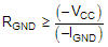
where
- –VCC is the maximum reverse battery voltage (typically –16 V).
- –IGND is the maximum reverse current the ground pin can withstand, which is available in the Absolute Maximum Ratings.
- Ground Diode: A diode is needed to block the reverse voltage, which also brings a ground shift (≈ 600 mV). Additionally, the diode must be ≈ 200-V reverse voltage for the ISO 7637 pulse 1 testing so that it does not get biased.