ZHCSLK6A July 2021 – December 2021 TPS1HC100-Q1
PRODUCTION DATA
- 1 特性
- 2 应用
- 3 说明
- 4 Revision History
- 5 Pin Configuration and Functions
- 6 Specifications
- 7 Parameter Measurement Information
-
8 Detailed Description
- 8.1 Overview
- 8.2 Functional Block Diagram
- 8.3
Feature Description
- 8.3.1 Accurate Current Sense
- 8.3.2 Programmable Current Limit
- 8.3.3 Inductive-Load Switching-Off Clamp
- 8.3.4
Full Protections and Diagnostics
- 8.3.4.1 Short-Circuit and Overload Protection
- 8.3.4.2 Open-Load and Short-to-Battery Detection
- 8.3.4.3 Short-to-Battery Detection
- 8.3.4.4 Reverse-Polarity and Battery Protection
- 8.3.4.5 Latch-Off Mode
- 8.3.4.6 Thermal Protection Behavior
- 8.3.4.7 UVLO Protection
- 8.3.4.8 Loss of GND Protection
- 8.3.4.9 Loss of Power Supply Protection
- 8.3.4.10 Reverse Current Protection
- 8.3.4.11 Protection for MCU I/Os
- 8.3.5 Diagnostic Enable Function
- 8.4 Device Functional Modes
- 9 Application and Implementation
- 10Power Supply Recommendations
- 11Layout
- 12Device and Documentation Support
- 13Mechanical, Packaging, and Orderable Information
8.3.3 Inductive-Load Switching-Off Clamp
When an inductive load is switching off, the output voltage is pulled down to negative, due to the inductance characteristics. The power FET can break down if the voltage is not clamped during the current-decay period. To protect the power FET in this situation, internally clamp the drain-to-source voltage, namely VDS,clamp, the clamp diode between the drain and gate.

During the current-decay period (TDECAY), the power FET is turned on for inductance-energy dissipation. Both the energy of the power supply (EBAT) and the load (ELOAD) are dissipated on the high-side power switch itself, which is called EHSD. If resistance is in series with inductance, some of the load energy is dissipated in the resistance.

From the high-side power switch’s view, EHSD equals the integration value during the current-decay period.
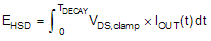
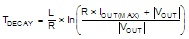
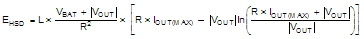
When R approximately equals 0, EHSD can be given simply as:
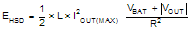
 Figure 8-7 Driving Inductive Load
 Figure 8-8 Inductive-Load Switching-Off Diagram
When switching off, battery energy and load energy are dissipated on the high-side power switch, which leads to the large thermal variation. For each high-side power switch, the upper limit of the maximum safe power dissipation depends on the device intrinsic capacity, ambient temperature, and board dissipation condition.
See Figure 8-9 for one dedicated inductance, 5 mH. If the maximum switching-off current is lower than the current value shown on the curve, the internal clamp function can be used for the demagnetization energy dissipation. If not, external free-wheeling circuitry is necessary for device protection.
 Figure 8-9 5-mH Maximum Demagnetization Curve