ZHCSNE6 August 2021 TPS1653
PRODUCTION DATA
- 1 特性
- 2 应用
- 3 说明
- 4 Revision History
- 5 Pin Configuration and Functions
- 6 Specifications
- 7 Parameter Measurement Information
-
8 Detailed Description
- 8.1 Overview
- 8.2 Functional Block Diagram
- 8.3
Feature Description
- 8.3.1 Hot Plug-In and In-Rush Current Control
- 8.3.2 Undervoltage Lockout (UVLO)
- 8.3.3 Overload and Short Circuit Protection
- 8.3.4 Current Monitoring Output (IMON)
- 8.3.5 FAULT Response (FLT)
- 8.3.6 Power Good Output (PGOOD)
- 8.3.7 IN, P_IN, OUT and GND Pins
- 8.3.8 Thermal Shutdown
- 8.3.9 Low Current Shutdown Control (SHDN)
- 8.3.10 Enable Input (EN)
- 8.4 Device Functional Modes
- 9 Application and Implementation
- 10Power Supply Recommendations
- 11Layout
- 12Device and Documentation Support
- 13Mechanical, Packaging, and Orderable Information
封装选项
机械数据 (封装 | 引脚)
散热焊盘机械数据 (封装 | 引脚)
订购信息
8.3.3.2.1 Start-Up With Short-Circuit On Output
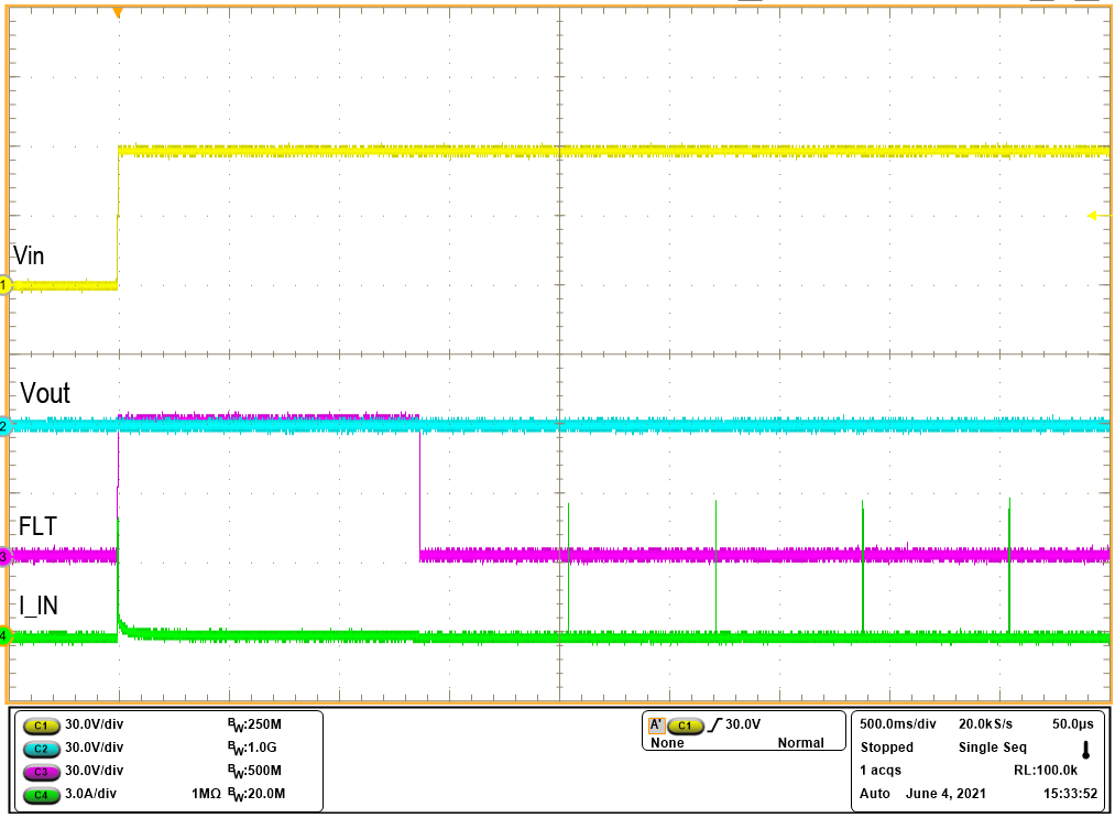
When the device is started with short-circuit on the output, the current begins to limit at I(OL). Due to high power dissipation of VIN × I(OL) within the device the junction temperature increases. Subsequently, the thermal regulation control loop limits the load current to regulate the junction temperature at T(J_REG), 145°C (typical) for a duration off t(Treg_timeout), 1.25 sec (typical). Subsequent operation of the device depends on the MODE configuration (Auto-Retry or latch OFF) setting as per Table 8-2. FLT gets asserted after t(Treg_timeout) and remains asserted till the output short-circuit is removed. Figure 8-6 illustrates the behavior of the device in this condition.

| VIN = 58 V | ILIM = 4.5 A |