ZHCSNE6 August 2021 TPS1653
PRODUCTION DATA
- 1 特性
- 2 应用
- 3 说明
- 4 Revision History
- 5 Pin Configuration and Functions
- 6 Specifications
- 7 Parameter Measurement Information
-
8 Detailed Description
- 8.1 Overview
- 8.2 Functional Block Diagram
- 8.3
Feature Description
- 8.3.1 Hot Plug-In and In-Rush Current Control
- 8.3.2 Undervoltage Lockout (UVLO)
- 8.3.3 Overload and Short Circuit Protection
- 8.3.4 Current Monitoring Output (IMON)
- 8.3.5 FAULT Response (FLT)
- 8.3.6 Power Good Output (PGOOD)
- 8.3.7 IN, P_IN, OUT and GND Pins
- 8.3.8 Thermal Shutdown
- 8.3.9 Low Current Shutdown Control (SHDN)
- 8.3.10 Enable Input (EN)
- 8.4 Device Functional Modes
- 9 Application and Implementation
- 10Power Supply Recommendations
- 11Layout
- 12Device and Documentation Support
- 13Mechanical, Packaging, and Orderable Information
封装选项
机械数据 (封装 | 引脚)
散热焊盘机械数据 (封装 | 引脚)
订购信息
10.1 Transient Protection
In case of short circuit and overload current limit, when the device interrupts current flow, input inductance generates a positive voltage spike on the input and output inductance generates a negative voltage spike on the output. The peak amplitude of voltage spikes (transients) depends on the value of inductance in series to the input or output of the device. These transients can exceed the Absolute Maximum Ratings of the device if steps are not taken to address the issue.
Typical methods for addressing transients include:
- Minimizing lead length and inductance into and out of the device
- Using large PCB GND plane
- Use of a Schottky diode across the output and GND to absorb negative spikes
- A low value ceramic capacitor (C(IN) to approximately 0.1 μF) to absorb the energy and dampen the transients.
The approximate value of input capacitance can be estimated with Equation 7.
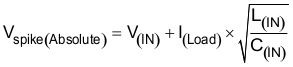
where
- V(IN) is the nominal supply voltage
- I(LOAD) is the load current
- L(IN) equals the effective inductance seen looking into the source
- C(IN) is the capacitance present at the input
Some applications may require additional Transient Voltage Suppressor (TVS) to prevent transients from exceeding the Absolute Maximum Ratings of the device. These transients can occur during positive and negative surge tests on the supply lines. In such applications, TI recommends to place at least 1 µF of input capacitor.
The circuit implementation with optional protection components (a ceramic capacitor, TVS and schottky diode) is shown in Figure 10-1.