ZHCSNE6 August 2021 TPS1653
PRODUCTION DATA
- 1 特性
- 2 应用
- 3 说明
- 4 Revision History
- 5 Pin Configuration and Functions
- 6 Specifications
- 7 Parameter Measurement Information
-
8 Detailed Description
- 8.1 Overview
- 8.2 Functional Block Diagram
- 8.3
Feature Description
- 8.3.1 Hot Plug-In and In-Rush Current Control
- 8.3.2 Undervoltage Lockout (UVLO)
- 8.3.3 Overload and Short Circuit Protection
- 8.3.4 Current Monitoring Output (IMON)
- 8.3.5 FAULT Response (FLT)
- 8.3.6 Power Good Output (PGOOD)
- 8.3.7 IN, P_IN, OUT and GND Pins
- 8.3.8 Thermal Shutdown
- 8.3.9 Low Current Shutdown Control (SHDN)
- 8.3.10 Enable Input (EN)
- 8.4 Device Functional Modes
- 9 Application and Implementation
- 10Power Supply Recommendations
- 11Layout
- 12Device and Documentation Support
- 13Mechanical, Packaging, and Orderable Information
封装选项
机械数据 (封装 | 引脚)
散热焊盘机械数据 (封装 | 引脚)
订购信息
8.3.1 Hot Plug-In and In-Rush Current Control
The devices are designed to control the inrush current upon insertion of a card into a live backplane or other "hot" power source. This limits the voltage sag on the backplane’s supply voltage and prevents unintended resets of the system power. The controlled start-up also helps to eliminate conductive and radiative interferences. An external capacitor connected from the dVdT pin to GND defines the slew rate of the output voltage at power-on. The fastest output slew rate of 24V/500 µs can be achieved by leaving dVdT pin floating. The inrush current can be calculated using Equation 1.
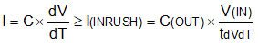
where
Figure 8-1 illustrates in-rush current control performance of the device during Hot Plug-In.

| CdVdT = 100 nF | COUT = 1000 µF | RILIM = 4.02 kΩ |