ZHCSNE6 August 2021 TPS1653
PRODUCTION DATA
- 1 特性
- 2 应用
- 3 说明
- 4 Revision History
- 5 Pin Configuration and Functions
- 6 Specifications
- 7 Parameter Measurement Information
-
8 Detailed Description
- 8.1 Overview
- 8.2 Functional Block Diagram
- 8.3
Feature Description
- 8.3.1 Hot Plug-In and In-Rush Current Control
- 8.3.2 Undervoltage Lockout (UVLO)
- 8.3.3 Overload and Short Circuit Protection
- 8.3.4 Current Monitoring Output (IMON)
- 8.3.5 FAULT Response (FLT)
- 8.3.6 Power Good Output (PGOOD)
- 8.3.7 IN, P_IN, OUT and GND Pins
- 8.3.8 Thermal Shutdown
- 8.3.9 Low Current Shutdown Control (SHDN)
- 8.3.10 Enable Input (EN)
- 8.4 Device Functional Modes
- 9 Application and Implementation
- 10Power Supply Recommendations
- 11Layout
- 12Device and Documentation Support
- 13Mechanical, Packaging, and Orderable Information
封装选项
机械数据 (封装 | 引脚)
散热焊盘机械数据 (封装 | 引脚)
订购信息
6.7 Typical Characteristics
–40°C ≤ TA = TJ ≤ +125°C, V(IN) = V(P_IN) = 24 V, V( SHDN) = 2 V, R(ILIM) = 30 kΩ, IMON = PGOOD = FLT = OPEN, C(OUT) = 1 μF, C(dVdT) = OPEN. (Unless stated otherwise)
 Figure 6-1 On-Resistance vs Temperature Across Load Current
Figure 6-3 Input
Supply Current vs Supply Voltage During Normal Operation
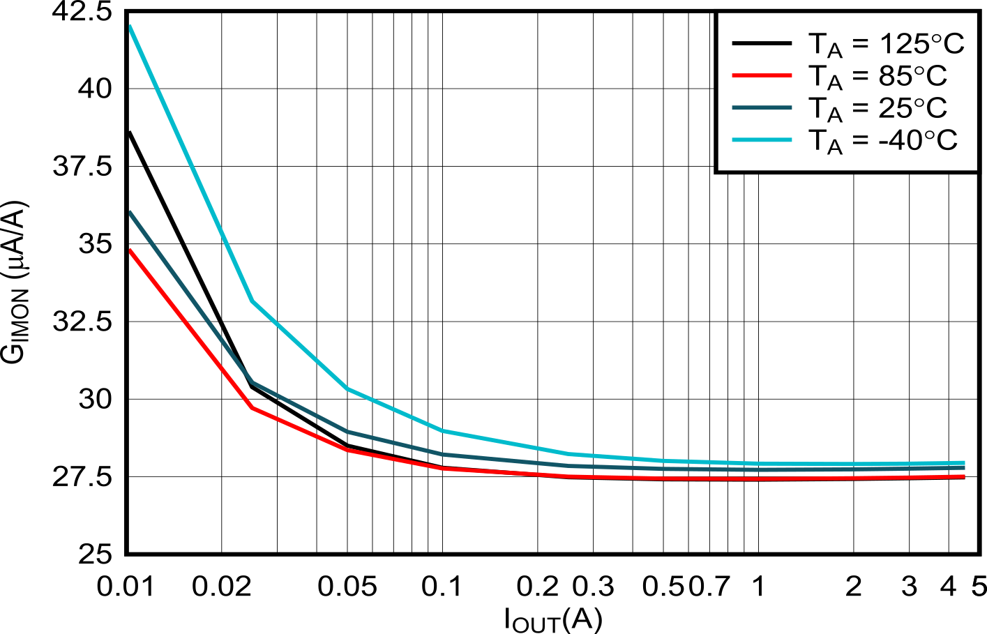
 Figure 6-5 Current Monitor Gain vs Output Current
| Taken on VQFN device with 95 cm2 copper connected to Exposed PAD |
Figure 6-2 Input
Supply Current vs Supply Voltage in Shutdown
Figure 6-4 Overload Current Limit vs Temperature

| IOUT = 4.5 A |
| Taken on HTSSOP with 110 cm2 copper connected to Exposed PAD |