ZHCS471C September 2011 – September 2019 TPL0501-100
PRODUCTION DATA.
- 1 特性
- 2 应用
- 3 说明
- 4 修订历史记录
- 5 Pin Configuration and Functions
- 6 Specifications
- 7 Detailed Description
- 8 Application and Implementation
- 9 Power Supply Recommendations
- 10Layout
- 11器件和文档支持
- 12机械、封装和可订购信息
封装选项
机械数据 (封装 | 引脚)
散热焊盘机械数据 (封装 | 引脚)
- DCN|8
订购信息
7.5.1 SPI Digital Interface
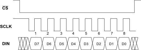
The TPL0501 uses a 3-wire SPI compatible serial data interface. This write-only interface has three inputs: chip-select (CS), data clock (SCLK), and data input (DIN). Drive CS low to enable the serial interface and clock data synchronously into the shift register on each SCLK rising edge. After loading data into the shift register, drive CS high to latch the data into the appropriate potentiometer control register and disable the serial interface. Keep CS low during the entire serial data stream to avoid corruption of the data.
Table 1. Register Map - Default Value 0x80
| BIT7 | BIT6 | BIT5 | BIT4 | BIT3 | BIT2 | BIT1 | BIT0 |
|---|---|---|---|---|---|---|---|
| MSB | LSB | ||||||
| D7 | D6 | D5 | D4 | D3 | D2 | D1 | D0 |
 Figure 15. SPI Write Sequence
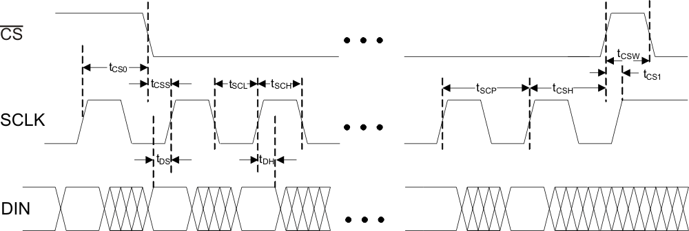
  Figure 16. Digital Interface Timing Diagram