ZHCSAT4D December   2012  – April 2017 TPD4E1U06

PRODUCTION DATA.  

  1. 特性
  2. 应用
  3. 说明
  4. 修订历史记录
  5. Pin Configuration and Functions
  6. Specifications
    1. 6.1 Absolute Maximum Ratings
    2. 6.2 ESD Ratings
    3. 6.3 ESD Ratings—IEC Specification
    4. 6.4 Recommended Operating Conditions
    5. 6.5 Thermal Information
    6. 6.6 Electrical Characteristics
    7. 6.7 Typical Characteristics
  7. Detailed Description
    1. 7.1 Overview
    2. 7.2 Functional Block Diagram
    3. 7.3 Feature Description
      1. 7.3.1 IEC 61000-4-2 Level 4 ESD Protection
      2. 7.3.2 IEC 61000-4-5 Surge Protection
      3. 7.3.3 IEC 61000-4-4 EFT Protection
      4. 7.3.4 IO Capacitance
      5. 7.3.5 DC Breakdown Voltage
      6. 7.3.6 Ultra Low Leakage Current
      7. 7.3.7 Low ESD Clamping Voltage
      8. 7.3.8 Industrial Temperature Range
      9. 7.3.9 Small, Easy-to-Route Packages
    4. 7.4 Device Functional Modes
  8. Application and Implementation
    1. 8.1 Application Information
    2. 8.2 Typical Application
      1. 8.2.1 Design Requirements
      2. 8.2.2 Detailed Design Procedure
        1. 8.2.2.1 Signal Range on Pins 1, 3, 4, or 6
        2. 8.2.2.2 Operating Frequency
      3. 8.2.3 Application Curve
  9. Power Supply Recommendations
  10. 10Layout
    1. 10.1 Layout Guidelines
    2. 10.2 Layout Example
  11. 11器件和文档支持
    1. 11.1 文档支持
      1. 11.1.1 相关文档
    2. 11.2 接收文档更新通知
    3. 11.3 社区资源
    4. 11.4 商标
    5. 11.5 静电放电警告
    6. 11.6 Glossary
  12. 12机械、封装和可订购信息

封装选项

机械数据 (封装 | 引脚)
散热焊盘机械数据 (封装 | 引脚)
订购信息

Layout

Layout Guidelines

  • The optimum placement is as close to the connector as possible.
    • EMI during an ESD event can couple from the trace being struck to other nearby unprotected traces, resulting in early system failures.
    • The PCB designer needs to minimize the possibility of EMI coupling by keeping any unprotected traces away from the protected traces which are between the TVS and the connector.
  • Route the protected traces as straight as possible.
  • Eliminate any sharp corners on the protected traces between the TVS and the connector by using rounded corners with the largest radii possible.
    • Electric fields tend to build up on corners, increasing EMI coupling.

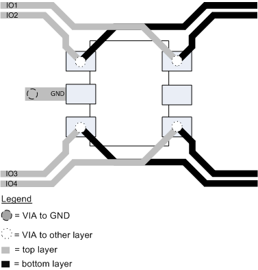
Layout Example

TPD4E1U06 TPD4E1U06-layout.gif Figure 12. PCB Layout Recommendation