ZHCSMX0B September 2019 – December 2020 TPA6304-Q1
PRODUCTION DATA
- 1 特性
- 2 应用
- 3 说明
- 4 Revision History
- 5 Pin Configuration and Functions
- 6 Specifications
- 7 Parameter measurement information
-
7 Detailed Description
- 7.1 Overview
- 7.2 Functional Block Diagram
- 7.3
Feature Description
- 7.3.1 Single-Ended Analog Inputs
- 7.3.2 Gain Control
- 7.3.3 Class-D Operation and Spread Spectrum Control
- 7.3.4 Gate Drive
- 7.3.5 Power FETs
- 7.3.6
Load Diagnostics
- 7.3.6.1
DC Load Diagnostics
- 7.3.6.1.1 Automatic DC Load Diagnostics at Device Initialization
- 7.3.6.1.2 Automatic DC Load Diagnostics During Hi-Z to MUTE or PLAY Transition
- 7.3.6.1.3 Manual Start of DC Load Diagnostics
- 7.3.6.1.4 Short-to-Ground
- 7.3.6.1.5 Short-to-Power
- 7.3.6.1.6 Shorted Load and Open Load
- 7.3.6.1.7 Line Output Diagnostics
- 7.3.6.2 AC Load Diagnostics
- 7.3.6.1
DC Load Diagnostics
- 7.3.7 Power Supply
- 7.3.8 Device Initialization and Power-On-Reset (POR)
- 7.3.9 Protection and Monitoring
- 7.3.10 Hardware Control Pins
- 7.4
Device Functional Modes
- 7.4.1 Internal Reporting Signals
- 7.4.2 Device States and Flags
- 7.4.3 Fault Events
- 7.4.4 Warning Events
- 7.5 Programming
- 7.6 Register Maps
- 8 Application Information Disclaimer
- 9 Power Supply Recommendations
- 10Layout
- 11Device and Documentation Support
5 Pin Configuration and Functions
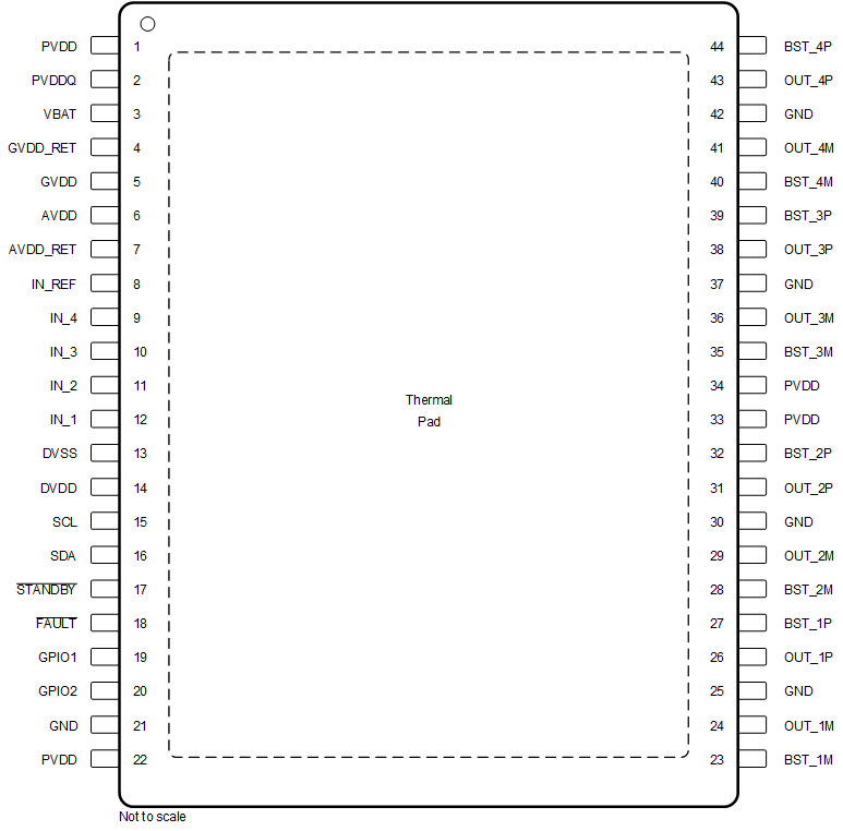
 Figure 5-1 DDV Package, 44-Pin HTSSOP, Top
View
Figure 5-1 DDV Package, 44-Pin HTSSOP, Top
ViewTable 5-1 Pin Functions
| PIN | TYPE(1) | DESCRIPTION | |
|---|---|---|---|
| NAME | NO. | ||
| AVDD | 6 | PWR | Voltage regulator bypass, derived from VBAT input pins. Connect 1 µF capacitor from AVDD (pin 6) to AVDD_RET (pin 7). |
| AVDD_RET | 7 | GND | AVDD voltage regulator return. Connect to ground. |
| BST_1M | 23 | PWR | Bootstrap capacitor connection pins for high-side gate driver |
| BST_1P | 27 | PWR | Bootstrap capacitor connection pins for high-side gate driver |
| BST_2M | 28 | PWR | Bootstrap capacitor connection pins for high-side gate driver |
| BST_2P | 32 | PWR | Bootstrap capacitor connection pins for high-side gate driver |
| BST_3M | 35 | PWR | Bootstrap capacitor connection pins for high-side gate driver |
| BST_3P | 39 | PWR | Bootstrap capacitor connection pins for high-side gate driver |
| BST_4M | 40 | PWR | Bootstrap capacitor connection pins for high-side gate driver |
| BST_4P | 44 | PWR | Bootstrap capacitor connection pins for high-side gate driver |
| DVDD | 14 | PWR | DVDD supply input. Connect 1 µF capacitor from DVDD to DVSS (pin 13). |
| DVSS | 13 | GND | DVDD ground reference. Connect to ground. |
| FAULT | 18 | DI/O | Reports a fault (active low, open drain), external pullup resistor determines I2C address during power on reset. |
| GND | 21, 25, 30, 37, 42 | GND | Ground |
| GPIO1 | 19 | DI/O | General purpose IO, function set by register programming. |
| GPIO2 | 20 | DI/O | General purpose IO, function set by register programming. |
| GVDD | 5 | PWR | Gate drive voltage regulator bypass for all output channels, derived from VBAT input pins. Connect 2.2µF capacitor to GVDD_RET (pin 4). |
| GVDD_RET | 4 | GND | Gate drive voltage regulator return. Connect to ground. |
| IN_1 | 12 | AI | Non-inverting input channel. Internally biased to AVDD/2. Connect to AC coupling capacitor. |
| IN_2 | 11 | AI | Non-inverting input channel. Internally biased to AVDD/2. Connect to AC coupling capacitor. |
| IN_3 | 10 | AI | Non-inverting input channel. Internally biased to AVDD/2. Connect to AC coupling capacitor. |
| IN_4 | 9 | AI | Non-inverting input channel. Internally biased to AVDD/2. Connect to AC coupling capacitor. |
| IN_REF | 8 | AI | Reference input voltage for IN_1, IN_2, IN_3, IN_4. Internally biased to AVDD/2. Connect to AC coupling capacitor. |
| OUT_1M | 24 | NO | Negative output for the channel |
| OUT_1P | 26 | PO | Positive output for the channel |
| OUT_2M | 29 | NO | Negative output for the channel |
| OUT_2P | 31 | PO | Positive output for the channel |
| OUT_3M | 36 | NO | Negative output for the channel |
| OUT_3P | 38 | PO | Positive output for the channel |
| OUT_4M | 41 | NO | Negative output for the channel |
| OUT_4P | 43 | PO | Positive output for the channel |
| PVDD | 1, 22, 33, 34 | PWR | PVDD voltage input carrying load currents (can be connected to battery). |
| PVDDQ | 2 | PWR | PVDD voltage input not loaded with load currents (can be connected to battery). |
| SCL | 15 | DI | I2C clock input |
| SDA | 16 | DI/O | I2C data input and output |
| STANDBY | 17 | DI | Enables low power standby state (active Low), 100-kΩ internal pulldown resistor. |
| VBAT | 3 | PWR | Battery voltage input |
| Thermal Pad | — | GND | Provides thermal connection for the device. Heatsink must be connected to GND. |
(1) AI = analog input, GND = ground, PWR = power, PO = positive output, NO =
negative output, DI = digital input, DO = digital output,
DI/O = digital input and output, NC = No Connection
DI/O = digital input and output, NC = No Connection