ZHCSHR9A March 2018 – June 2018 TPA3138D2
PRODUCTION DATA.
- 1 特性
- 2 应用
- 3 说明
- 4 修订历史记录
- 5 Device Comparison Table
- 6 Pin Configuration and Functions
- 7 Specifications
- 8 Parameter Measurement Information
-
9 Detailed Description
- 9.1 Overview
- 9.2 Functional Block Diagram
- 9.3
Feature Description
- 9.3.1 Analog Gain
- 9.3.2 SD/FAULT Operation
- 9.3.3 PLIMIT
- 9.3.4 Spread Spectrum and De-Phase Control
- 9.3.5 GVDD Supply
- 9.3.6 DC Detect
- 9.3.7 PBTL Select
- 9.3.8 Short-Circuit Protection and Automatic Recovery Feature
- 9.3.9 Over-Temperature Protection (OTP)
- 9.3.10 Over-Voltage Protection (OVP)
- 9.3.11 Under-Voltage Protection (UVP)
- 9.4 Device Functional Modes
-
10Application and Implementation
- 10.1 Application Information
- 10.2
Typical Applications
- 10.2.1 Design Requirements
- 10.2.2
Detailed Design Procedure
- 10.2.2.1 Ferrite Bead Filter Considerations
- 10.2.2.2 Efficiency: LC Filter Required with the Traditional Class-D Modulation Scheme
- 10.2.2.3 When to Use an Output Filter for EMI Suppression
- 10.2.2.4 Input Resistance
- 10.2.2.5 Input Capacitor, Ci
- 10.2.2.6 BSN and BSP Capacitors
- 10.2.2.7 Differential Inputs
- 10.2.2.8 Using Low-ESR Capacitors
- 10.2.3 Application Performance Curves
- 11Power Supply Recommendations
- 12Layout
- 13器件和文档支持
- 14机械、封装和可订购信息
9.4.1 MODE_SEL = LOW: BD Modulation
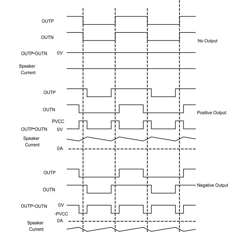
This is a modulation scheme that allows operation without the classic LC reconstruction filter when the amp is driving an inductive load with short speaker wires. Each output is switching from 0 volts to the supply voltage. The OUTPx and OUTNx are in phase with each other with no input so that there is little or no current in the speaker. The duty cycle of OUTPx is greater than 50% and OUTNx is less than 50% for positive output voltages. The duty cycle of OUTPx is less than 50% and OUTNx is greater than 50% for negative output voltages. The voltage across the load sits at 0 V throughout most of the switching period, reducing the switching current, which reduces any I2R losses in the load.
 Figure 18. BD Mode Modulation