ZHCSHR9A March 2018 – June 2018 TPA3138D2
PRODUCTION DATA.
- 1 特性
- 2 应用
- 3 说明
- 4 修订历史记录
- 5 Device Comparison Table
- 6 Pin Configuration and Functions
- 7 Specifications
- 8 Parameter Measurement Information
-
9 Detailed Description
- 9.1 Overview
- 9.2 Functional Block Diagram
- 9.3
Feature Description
- 9.3.1 Analog Gain
- 9.3.2 SD/FAULT Operation
- 9.3.3 PLIMIT
- 9.3.4 Spread Spectrum and De-Phase Control
- 9.3.5 GVDD Supply
- 9.3.6 DC Detect
- 9.3.7 PBTL Select
- 9.3.8 Short-Circuit Protection and Automatic Recovery Feature
- 9.3.9 Over-Temperature Protection (OTP)
- 9.3.10 Over-Voltage Protection (OVP)
- 9.3.11 Under-Voltage Protection (UVP)
- 9.4 Device Functional Modes
-
10Application and Implementation
- 10.1 Application Information
- 10.2
Typical Applications
- 10.2.1 Design Requirements
- 10.2.2
Detailed Design Procedure
- 10.2.2.1 Ferrite Bead Filter Considerations
- 10.2.2.2 Efficiency: LC Filter Required with the Traditional Class-D Modulation Scheme
- 10.2.2.3 When to Use an Output Filter for EMI Suppression
- 10.2.2.4 Input Resistance
- 10.2.2.5 Input Capacitor, Ci
- 10.2.2.6 BSN and BSP Capacitors
- 10.2.2.7 Differential Inputs
- 10.2.2.8 Using Low-ESR Capacitors
- 10.2.3 Application Performance Curves
- 11Power Supply Recommendations
- 12Layout
- 13器件和文档支持
- 14机械、封装和可订购信息
7.7 Typical Characteristics
All measurements taken at audio frequency = 1 kHz, closed-loop gain = 26 dB, BD mode, T A= 25°C, AES17 filter using the TPA3138D2EVM, unless otherwise noted.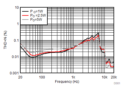
| AVCC=PVCC = 12 V, Load = 6 Ω + 47 µH, 1 W, 2.5 W, 5 W |
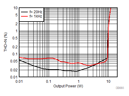
| AVCC=PVCC = 12 V, Load = 6 Ω + 47 µH, 20 Hz, 1 kHz |
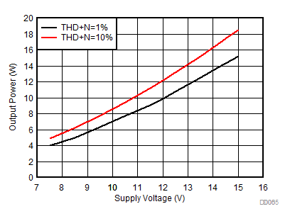
| AVCC=PVCC = 7.5 V to 15 V, Load = 6 Ω + 47 µH |
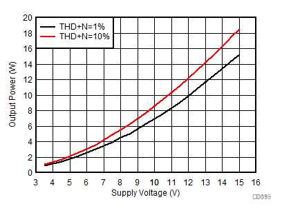
| AVCC=PVCC = 3.5 V to 15 V, Load = 6 Ω + 47 µH, Low-Idle-Current 1SPW Mode |
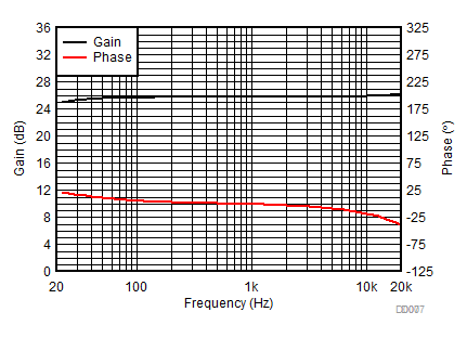
1.
Figure 9. Gain and Phase vs Frequency (BTL) | AVCC= PVCC = 12 V, Load = 6 Ω + 47 µH |

| AVCC=PVCC= 13 V, 14.4 V, Load = 8 Ω + 66 µH |
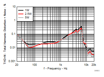
| AVCC=PVCC = 13 V, Load = 4 Ω + 33 µH, 1 W, 2.5 W, 5 W |
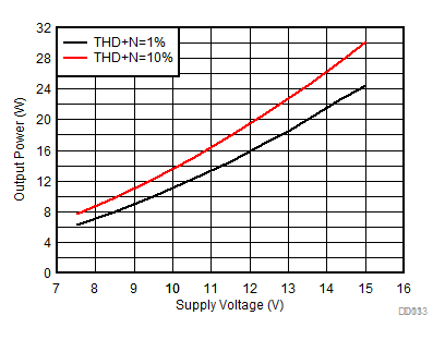
| AVCC=PVCC = 7.5 V to 14.4 V, Load = 4 Ω + 33 µH |
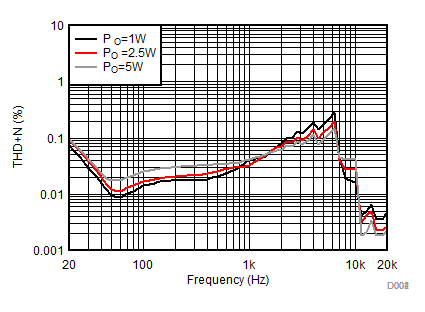
| AVCC=PVCC = 13 V, Load = 8 Ω + 66 µH, 1 W, 2.5 W, 5 W |

| AVCC=PVCC = 13 V, Load = 8 Ω + 66 µH, 20 Hz, 1 kHz |
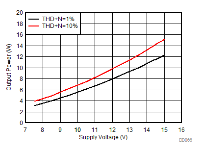
| AVCC=PVCC = 7.5 V to 15 V, Load = 8 Ω + 66 µH |
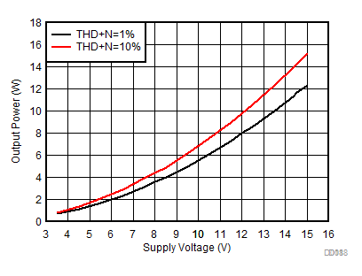
1.
Figure 8. Output Power vs Supply Voltage (BTL) | AVCC= PVCC = 3.5 V to 15 V, Load = 8 Ω + 66 µH, Low-Idle-Current 1SPW Mode |
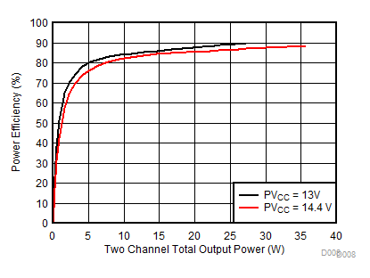
| AVCC=PVCC = 12 V, 14.4 V, Load = 6 Ω + 47 µH |
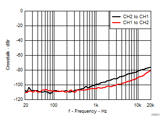
| AVCC=PVCC = 12 V, 1 W, Load = 6 Ω + 47 µH |
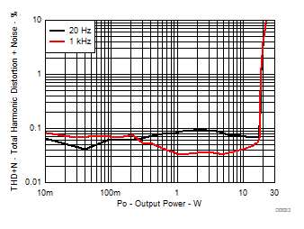
| AVCC=PVCC = 13 V, Load = 4 Ω + 33 µH, 20 Hz, 1 kHz |
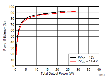
| AVCC=PVCC = 13 V, 14.4 V, Load = 4 Ω + 33 µH | ||