ZHCSKY9E March 2020 – October 2022 TMUX1308 , TMUX1309
PRODUCTION DATA
- 1 特性
- 2 应用
- 3 说明
- 4 Revision History
- 5 Device Comparison Table
- 6 Pin Configuration and Functions
-
7 Specifications
- 7.1 Absolute Maximum Ratings
- 7.2 ESD Ratings
- 7.3 Recommended Operating Conditions
- 7.4 Thermal Information: TMUX1308
- 7.5 Thermal Information: TMUX1309
- 7.6 Electrical Characteristics
- 7.7 Logic and Dynamic Characteristics
- 7.8 Timing Characteristics
- 7.9 Injection Current Coupling
- 7.10 Typical Characteristics
- 8 Parameter Measurement Information
-
9 Detailed Description
- 9.1 Overview
- 9.2 Functional Block Diagram
- 9.3
Feature Description
- 9.3.1 Bidirectional Operation
- 9.3.2 Rail-to-Rail Operation
- 9.3.3 1.8 V Logic Compatible Inputs
- 9.3.4 Fail-Safe Logic
- 9.3.5
Injection Current Control
- 9.3.5.1 TMUX13xx is Powered, Channel is Unselected, and the Input Signal is Greater Than VDD (VDD = 5 V, VINPUT = 5.5 V)
- 9.3.5.2 TMUX13xx is Powered, Channel is Selected, and the Input Signal is Greater Than VDD (VDD = 5 V, VINPUT = 5.5 V)
- 9.3.5.3 TMUX13xx is Unpowered and the Input Signal has a Voltage Present (VDD = 0 V, VINPUT = 3 V)
- 9.4 Device Functional Modes
- 9.5 Truth Tables
- 10Application and Implementation
- 11Power Supply Recommendations
- 12Layout
- 13Device and Documentation Support
- 14Mechanical, Packaging, and Orderable Information
封装选项
机械数据 (封装 | 引脚)
散热焊盘机械数据 (封装 | 引脚)
- BQB|16
订购信息
10.2 Typical Application
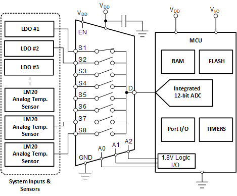
One useful application that takes advantage of the TMUX13xx features is multiplexing various signals into an ADC that is integrated into an MCU. Utilizing an integrated ADC in an MCU allows a system to minimize cost with a potential tradeoff of system performance when compared to an external ADC. The multiplexer allows for multiple inputs or sensors to be monitored with a single ADC pin of the device, which is critical in systems with limited I/O. The TMUX1309 is suitable for a similar design example using differential signals, or as two 4:1 multiplexers.
 Figure 10-1 Multiplexing Signals to Integrated ADC