ZHCSGV6F June 2009 – January 2017 TMS320C6742
PRODUCTION DATA.
- 1器件概述
- 2Revision History
-
3Device Comparison
- 3.1 Device Characteristics
- 3.2 Device Compatibility
- 3.3 DSP Subsystem
- 3.4 Memory Map Summary
- 3.5 Pin Assignments
- 3.6 Pin Multiplexing Control
- 3.7
Terminal Functions
- 3.7.1 Device Reset, NMI and JTAG
- 3.7.2 High-Frequency Oscillator and PLL
- 3.7.3 Real-Time Clock and 32-kHz Oscillator
- 3.7.4 DEEPSLEEP Power Control
- 3.7.5 External Memory Interface A (EMIFA)
- 3.7.6 DDR2/mDDR Controller
- 3.7.7 Serial Peripheral Interface Modules (SPI)
- 3.7.8 Enhanced Capture/Auxiliary PWM Modules (eCAP0)
- 3.7.9 Enhanced Pulse Width Modulators (eHRPWM)
- 3.7.10 Boot
- 3.7.11 Universal Asynchronous Receiver/Transmitters (UART0)
- 3.7.12 Inter-Integrated Circuit Modules(I2C0)
- 3.7.13 Timers
- 3.7.14 Multichannel Audio Serial Ports (McASP)
- 3.7.15 Multichannel Buffered Serial Ports (McBSP)
- 3.7.16 Universal Host-Port Interface (UHPI)
- 3.7.17 General Purpose Input Output
- 3.7.18 Reserved and No Connect
- 3.7.19 Supply and Ground
- 3.8 Unused Pin Configurations
- 4Device Configuration
-
5Specifications
- 5.1 Absolute Maximum Ratings Over Operating Junction Temperature Range (Unless Otherwise Noted)
- 5.2 Handling Ratings
- 5.3 Recommended Operating Conditions
- 5.4 Notes on Recommended Power-On Hours (POH)
- 5.5 Electrical Characteristics Over Recommended Ranges of Supply Voltage and Operating Junction Temperature (Unless Otherwise Noted)
-
6Peripheral Information and Electrical Specifications
- 6.1 Parameter Information
- 6.2 Recommended Clock and Control Signal Transition Behavior
- 6.3 Power Supplies
- 6.4 Reset
- 6.5 Crystal Oscillator or External Clock Input
- 6.6 Clock PLLs
- 6.7 Interrupts
- 6.8 Power and Sleep Controller (PSC)
- 6.9 Enhanced Direct Memory Access Controller (EDMA3)
- 6.10 External Memory Interface A (EMIFA)
- 6.11
DDR2/mDDR Memory Controller
- 6.11.1 DDR2/mDDR Memory Controller Electrical Data/Timing
- 6.11.2 DDR2/mDDR Memory Controller Register Description(s)
- 6.11.3
DDR2/mDDR Interface
- 6.11.3.1 DDR2/mDDR Interface Schematic
- 6.11.3.2 Compatible JEDEC DDR2/mDDR Devices
- 6.11.3.3 PCB Stackup
- 6.11.3.4 Placement
- 6.11.3.5 DDR2/mDDR Keep Out Region
- 6.11.3.6 Bulk Bypass Capacitors
- 6.11.3.7 High-Speed Bypass Capacitors
- 6.11.3.8 Net Classes
- 6.11.3.9 DDR2/mDDR Signal Termination
- 6.11.3.10 VREF Routing
- 6.11.3.11 DDR2/mDDR CK and ADDR_CTRL Routing
- 6.11.3.12 DDR2/mDDR Boundary Scan Limitations
- 6.12 Memory Protection Units
- 6.13 Multichannel Audio Serial Port (McASP)
- 6.14
Multichannel Buffered Serial Port (McBSP)
- 6.14.1 McBSP Peripheral Register Description(s)
- 6.14.2
McBSP Electrical Data/Timing
- 6.14.2.1
Multichannel Buffered Serial Port (McBSP) Timing
- Table 6-47 Timing Requirements for McBSP1 [1.2V, 1.1V] (see )
- Table 6-48 Timing Requirements for McBSP1 [1.0V] (see )
- Table 6-49 Switching Characteristics for McBSP1 [1.2V, 1.1V] (see )
- Table 6-50 Switching Characteristics for McBSP1 [1.0V] (see )
- Table 6-51 Timing Requirements for McBSP1 FSR When GSYNC = 1 (see )
- 6.14.2.1
Multichannel Buffered Serial Port (McBSP) Timing
- 6.15 Serial Peripheral Interface Ports (SPI1)
- 6.16 Inter-Integrated Circuit Serial Ports (I2C)
- 6.17 Universal Asynchronous Receiver/Transmitter (UART)
- 6.18 Host-Port Interface (UHPI)
- 6.19 Enhanced Capture (eCAP) Peripheral
- 6.20 Enhanced High-Resolution Pulse-Width Modulator (eHRPWM)
- 6.21 Timers
- 6.22 Real Time Clock (RTC)
- 6.23 General-Purpose Input/Output (GPIO)
- 6.24 Emulation Logic
- 7Device and Documentation Support
- 8Mechanical Packaging and Orderable Information
6.20 Enhanced High-Resolution Pulse-Width Modulator (eHRPWM)
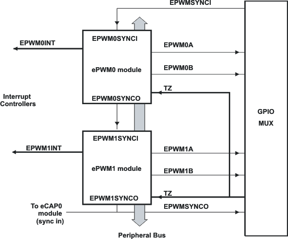
The device contains two enhanced PWM Modules (eHRPWM). Figure 6-46 shows a block diagram of multiple eHRPWM modules. Figure 6-46 shows the signal interconnections with the eHRPWM.
 Figure 6-46 Multiple PWM Modules in a C6742 System
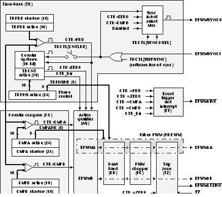
 Figure 6-47 eHRPWM Sub-Modules Showing Critical Internal Signal Interconnections
Table 6-74 eHRPWM Module Control and Status Registers Grouped by Submodule
| eHRPWM0
BYTE ADDRESS |
eHRPWM1
BYTE ADDRESS |
ACRONYM | SHADOW | REGISTER DESCRIPTION |
|---|---|---|---|---|
| Time-Base Submodule Registers | ||||
| 0x01F0 0000 | 0x01F0 2000 | TBCTL | No | Time-Base Control Register |
| 0x01F0 0002 | 0x01F0 2002 | TBSTS | No | Time-Base Status Register |
| 0x01F0 0004 | 0x01F0 2004 | TBPHSHR | No | Extension for HRPWM Phase Register(1) |
| 0x01F0 0006 | 0x01F0 2006 | TBPHS | No | Time-Base Phase Register |
| 0x01F0 0008 | 0x01F0 2008 | TBCNT | No | Time-Base Counter Register |
| 0x01F0 000A | 0x01F0 200A | TBPRD | Yes | Time-Base Period Register |
| Counter-Compare Submodule Registers | ||||
| 0x01F0 000E | 0x01F0 200E | CMPCTL | No | Counter-Compare Control Register |
| 0x01F0 0010 | 0x01F0 2010 | CMPAHR | No | Extension for HRPWM Counter-Compare A Register(1) |
| 0x01F0 0012 | 0x01F0 2012 | CMPA | Yes | Counter-Compare A Register |
| 0x01F0 0014 | 0x01F0 2014 | CMPB | Yes | Counter-Compare B Register |
| Action-Qualifier Submodule Registers | ||||
| 0x01F0 0016 | 0x01F0 2016 | AQCTLA | No | Action-Qualifier Control Register for Output A (eHRPWMxA) |
| 0x01F0 0018 | 0x01F0 2018 | AQCTLB | No | Action-Qualifier Control Register for Output B (eHRPWMxB) |
| 0x01F0 001A | 0x01F0 201A | AQSFRC | No | Action-Qualifier Software Force Register |
| 0x01F0 001C | 0x01F0 201C | AQCSFRC | Yes | Action-Qualifier Continuous S/W Force Register Set |
| Dead-Band Generator Submodule Registers | ||||
| 0x01F0 001E | 0x01F0 201E | DBCTL | No | Dead-Band Generator Control Register |
| 0x01F0 0020 | 0x01F0 2020 | DBRED | No | Dead-Band Generator Rising Edge Delay Count Register |
| 0x01F0 0022 | 0x01F0 2022 | DBFED | No | Dead-Band Generator Falling Edge Delay Count Register |
| PWM-Chopper Submodule Registers | ||||
| 0x01F0 003C | 0x01F0 203C | PCCTL | No | PWM-Chopper Control Register |
| Trip-Zone Submodule Registers | ||||
| 0x01F0 0024 | 0x01F0 2024 | TZSEL | No | Trip-Zone Select Register |
| 0x01F0 0028 | 0x01F0 2028 | TZCTL | No | Trip-Zone Control Register |
| 0x01F0 002A | 0x01F0 202A | TZEINT | No | Trip-Zone Enable Interrupt Register |
| 0x01F0 002C | 0x01F0 202C | TZFLG | No | Trip-Zone Flag Register |
| 0x01F0 002E | 0x01F0 202E | TZCLR | No | Trip-Zone Clear Register |
| 0x01F0 0030 | 0x01F0 2030 | TZFRC | No | Trip-Zone Force Register |
| Event-Trigger Submodule Registers | ||||
| 0x01F0 0032 | 0x01F0 2032 | ETSEL | No | Event-Trigger Selection Register |
| 0x01F0 0034 | 0x01F0 2034 | ETPS | No | Event-Trigger Pre-Scale Register |
| 0x01F0 0036 | 0x01F0 2036 | ETFLG | No | Event-Trigger Flag Register |
| 0x01F0 0038 | 0x01F0 2038 | ETCLR | No | Event-Trigger Clear Register |
| 0x01F0 003A | 0x01F0 203A | ETFRC | No | Event-Trigger Force Register |
| High-Resolution PWM (HRPWM) Submodule Registers | ||||
| 0x01F0 1040 | 0x01F0 3040 | HRCNFG | No | HRPWM Configuration Register (1) |
(1) These registers are only available on eHRPWM instances that include the high-resolution PWM (HRPWM) extension; otherwise, these locations are reserved.