ZHCSGV6F June 2009 – January 2017 TMS320C6742
PRODUCTION DATA.
- 1器件概述
- 2Revision History
-
3Device Comparison
- 3.1 Device Characteristics
- 3.2 Device Compatibility
- 3.3 DSP Subsystem
- 3.4 Memory Map Summary
- 3.5 Pin Assignments
- 3.6 Pin Multiplexing Control
- 3.7
Terminal Functions
- 3.7.1 Device Reset, NMI and JTAG
- 3.7.2 High-Frequency Oscillator and PLL
- 3.7.3 Real-Time Clock and 32-kHz Oscillator
- 3.7.4 DEEPSLEEP Power Control
- 3.7.5 External Memory Interface A (EMIFA)
- 3.7.6 DDR2/mDDR Controller
- 3.7.7 Serial Peripheral Interface Modules (SPI)
- 3.7.8 Enhanced Capture/Auxiliary PWM Modules (eCAP0)
- 3.7.9 Enhanced Pulse Width Modulators (eHRPWM)
- 3.7.10 Boot
- 3.7.11 Universal Asynchronous Receiver/Transmitters (UART0)
- 3.7.12 Inter-Integrated Circuit Modules(I2C0)
- 3.7.13 Timers
- 3.7.14 Multichannel Audio Serial Ports (McASP)
- 3.7.15 Multichannel Buffered Serial Ports (McBSP)
- 3.7.16 Universal Host-Port Interface (UHPI)
- 3.7.17 General Purpose Input Output
- 3.7.18 Reserved and No Connect
- 3.7.19 Supply and Ground
- 3.8 Unused Pin Configurations
- 4Device Configuration
-
5Specifications
- 5.1 Absolute Maximum Ratings Over Operating Junction Temperature Range (Unless Otherwise Noted)
- 5.2 Handling Ratings
- 5.3 Recommended Operating Conditions
- 5.4 Notes on Recommended Power-On Hours (POH)
- 5.5 Electrical Characteristics Over Recommended Ranges of Supply Voltage and Operating Junction Temperature (Unless Otherwise Noted)
-
6Peripheral Information and Electrical Specifications
- 6.1 Parameter Information
- 6.2 Recommended Clock and Control Signal Transition Behavior
- 6.3 Power Supplies
- 6.4 Reset
- 6.5 Crystal Oscillator or External Clock Input
- 6.6 Clock PLLs
- 6.7 Interrupts
- 6.8 Power and Sleep Controller (PSC)
- 6.9 Enhanced Direct Memory Access Controller (EDMA3)
- 6.10 External Memory Interface A (EMIFA)
- 6.11
DDR2/mDDR Memory Controller
- 6.11.1 DDR2/mDDR Memory Controller Electrical Data/Timing
- 6.11.2 DDR2/mDDR Memory Controller Register Description(s)
- 6.11.3
DDR2/mDDR Interface
- 6.11.3.1 DDR2/mDDR Interface Schematic
- 6.11.3.2 Compatible JEDEC DDR2/mDDR Devices
- 6.11.3.3 PCB Stackup
- 6.11.3.4 Placement
- 6.11.3.5 DDR2/mDDR Keep Out Region
- 6.11.3.6 Bulk Bypass Capacitors
- 6.11.3.7 High-Speed Bypass Capacitors
- 6.11.3.8 Net Classes
- 6.11.3.9 DDR2/mDDR Signal Termination
- 6.11.3.10 VREF Routing
- 6.11.3.11 DDR2/mDDR CK and ADDR_CTRL Routing
- 6.11.3.12 DDR2/mDDR Boundary Scan Limitations
- 6.12 Memory Protection Units
- 6.13 Multichannel Audio Serial Port (McASP)
- 6.14
Multichannel Buffered Serial Port (McBSP)
- 6.14.1 McBSP Peripheral Register Description(s)
- 6.14.2
McBSP Electrical Data/Timing
- 6.14.2.1
Multichannel Buffered Serial Port (McBSP) Timing
- Table 6-47 Timing Requirements for McBSP1 [1.2V, 1.1V] (see )
- Table 6-48 Timing Requirements for McBSP1 [1.0V] (see )
- Table 6-49 Switching Characteristics for McBSP1 [1.2V, 1.1V] (see )
- Table 6-50 Switching Characteristics for McBSP1 [1.0V] (see )
- Table 6-51 Timing Requirements for McBSP1 FSR When GSYNC = 1 (see )
- 6.14.2.1
Multichannel Buffered Serial Port (McBSP) Timing
- 6.15 Serial Peripheral Interface Ports (SPI1)
- 6.16 Inter-Integrated Circuit Serial Ports (I2C)
- 6.17 Universal Asynchronous Receiver/Transmitter (UART)
- 6.18 Host-Port Interface (UHPI)
- 6.19 Enhanced Capture (eCAP) Peripheral
- 6.20 Enhanced High-Resolution Pulse-Width Modulator (eHRPWM)
- 6.21 Timers
- 6.22 Real Time Clock (RTC)
- 6.23 General-Purpose Input/Output (GPIO)
- 6.24 Emulation Logic
- 7Device and Documentation Support
- 8Mechanical Packaging and Orderable Information
6.19 Enhanced Capture (eCAP) Peripheral
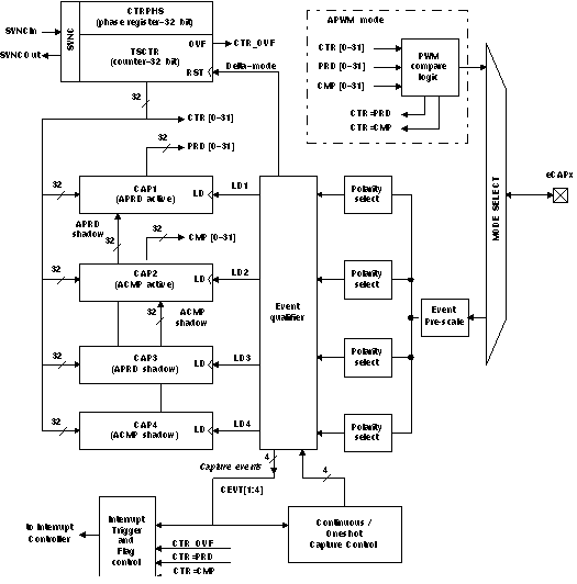
The device contains up to three enhanced capture (eCAP) modules. Figure 6-45 shows a functional block diagram of a module.
Uses for ECAP include:
- Speed measurements of rotating machinery (e.g. toothed sprockets sensed via Hall sensors)
- Elapsed time measurements between position sensor triggers
- Period and duty cycle measurements of pulse train signals
- Decoding current or voltage amplitude derived from duty cycle encoded current/voltage sensors
The ECAP module described in this specification includes the following features:
- 32 bit time base
- 4 event time-stamp registers (each 32 bits)
- Edge polarity selection for up to 4 sequenced time-stamp capture events
- Interrupt on either of the 4 events
- Single shot capture of up to 4 event time-stamps
- Continuous mode capture of time-stamps in a 4 deep circular buffer
- Absolute time-stamp capture
- Difference mode time-stamp capture
- All the above resources are dedicated to a single input pin
The eCAP modules are clocked at the ASYNC3 clock domain rate.
 Figure 6-45 eCAP Functional Block Diagram
Table 6-71 is the list of the ECAP registers.
Table 6-71 ECAPx Configuration Registers
| ECAP0
BYTE ADDRESS |
ECAP1
BYTE ADDRESS |
ECAP2
BYTE ADDRESS |
ACRONYM | DESCRIPTION |
|---|---|---|---|---|
| 0x01F0 6000 | 0x01F0 7000 | 0x01F0 8000 | TSCTR | Time-Stamp Counter |
| 0x01F0 6004 | 0x01F0 7004 | 0x01F0 8004 | CTRPHS | Counter Phase Offset Value Register |
| 0x01F0 6008 | 0x01F0 7008 | 0x01F0 8008 | CAP1 | Capture 1 Register |
| 0x01F0 600C | 0x01F0 700C | 0x01F0 800C | CAP2 | Capture 2 Register |
| 0x01F0 6010 | 0x01F0 7010 | 0x01F0 8010 | CAP3 | Capture 3 Register |
| 0x01F0 6014 | 0x01F0 7014 | 0x01F0 8014 | CAP4 | Capture 4 Register |
| 0x01F0 6028 | 0x01F0 7028 | 0x01F0 8028 | ECCTL1 | Capture Control Register 1 |
| 0x01F0 602A | 0x01F0 702A | 0x01F0 802A | ECCTL2 | Capture Control Register 2 |
| 0x01F0 602C | 0x01F0 702C | 0x01F0 802C | ECEINT | Capture Interrupt Enable Register |
| 0x01F0 602E | 0x01F0 702E | 0x01F0 802E | ECFLG | Capture Interrupt Flag Register |
| 0x01F0 6030 | 0x01F0 7030 | 0x01F0 8030 | ECCLR | Capture Interrupt Clear Register |
| 0x01F0 6032 | 0x01F0 7032 | 0x01F0 8032 | ECFRC | Capture Interrupt Force Register |
| 0x01F0 605C | 0x01F0 705C | 0x01F0 805C | REVID | Revision ID |
Table 6-72 shows the eCAP timing requirement and Table 6-73 shows the eCAP switching characteristics.