ZHCSDR5B March 2012 – April 2015 TMS320C6654
PRODUCTION DATA.
- 1 C6654 特性和描述
- 2 修订历史记录
-
3 Device Overview
- 3.1 Device Characteristics
- 3.2 DSP Core Description
- 3.3 Memory Map Summary
- 3.4 Boot Sequence
- 3.5
Boot Modes Supported and PLL Settings
- 3.5.1 Boot Device Field
- 3.5.2 Device Configuration Field
- 3.5.3
Boot Parameter Table
- 3.5.3.1 Sleep / XIP Mode Parameter Table
- 3.5.3.2 SRIO Mode Boot Parameter Table
- 3.5.3.3 Ethernet Mode Boot Parameter Table
- 3.5.3.4 NAND Mode Boot Parameter Table
- 3.5.3.5 PCIE Mode Boot Parameter Table
- 3.5.3.6 I2C Mode Boot Parameter Table
- 3.5.3.7 SPI Mode Boot Parameter Table
- 3.5.3.8 Hyperlink Mode Boot Parameter Table
- 3.5.3.9 UART Mode Boot Parameter Table
- 3.6 PLL Boot Configuration Settings
- 3.7 Second-Level Bootloaders
- 3.8 Terminals
- 3.9 Terminal Functions
-
4 Device Configuration
- 4.1 Device Configuration at Device Reset
- 4.2 Peripheral Selection After Device Reset
- 4.3
Device State Control Registers
- 4.3.1 Device Status Register
- 4.3.2 Device Configuration Register
- 4.3.3 JTAG ID (JTAGID) Register Description
- 4.3.4 Kicker Mechanism (KICK0 and KICK1) Register
- 4.3.5 LRESETNMI PIN Status (LRSTNMIPINSTAT) Register
- 4.3.6 LRESETNMI PIN Status Clear (LRSTNMIPINSTAT_CLR) Register
- 4.3.7 Reset Status (RESET_STAT) Register
- 4.3.8 Reset Status Clear (RESET_STAT_CLR) Register
- 4.3.9 Boot Complete (BOOTCOMPLETE) Register
- 4.3.10 Power State Control (PWRSTATECTL) Register
- 4.3.11 NMI Event Generation to CorePac (NMIGRx) Register
- 4.3.12 IPC Generation (IPCGRx) Registers
- 4.3.13 IPC Acknowledgement (IPCARx) Registers
- 4.3.14 IPC Generation Host (IPCGRH) Register
- 4.3.15 IPC Acknowledgement Host (IPCARH) Register
- 4.3.16 Timer Input Selection Register (TINPSEL)
- 4.3.17 Timer Output Selection Register (TOUTPSEL)
- 4.3.18 Reset Mux (RSTMUXx) Register
- 4.3.19 Device Speed (DEVSPEED) Register
- 4.3.20 Pin Control 0 (PIN_CONTROL_0) Register
- 4.3.21 Pin Control 1 (PIN_CONTROL_1) Register
- 4.3.22 uPP Clock Source (UPP_CLOCK) Register
- 4.4 Pullup/Pulldown Resistors
- 5 System Interconnect
- 6 C66x CorePac
- 7 Device Operating Conditions
-
8 Peripheral Information and Electrical Specifications
- 8.1 Recommended Clock and Control Signal Transition Behavior
- 8.2 Power Supplies
- 8.3 Power Sleep Controller (PSC)
- 8.4 Reset Controller
- 8.5
Main PLL and PLL Controller
- 8.5.1 Main PLL Controller Device-Specific Information
- 8.5.2
PLL Controller Memory Map
- 8.5.2.1 PLL Secondary Control Register (SECCTL)
- 8.5.2.2 PLL Controller Divider Register (PLLDIV2, PLLDIV5, PLLDIV8)
- 8.5.2.3 PLL Controller Clock Align Control Register (ALNCTL)
- 8.5.2.4 PLLDIV Divider Ratio Change Status Register (DCHANGE)
- 8.5.2.5 SYSCLK Status Register (SYSTAT)
- 8.5.2.6 Reset Type Status Register (RSTYPE)
- 8.5.2.7 Reset Control Register (RSTCTRL)
- 8.5.2.8 Reset Configuration Register (RSTCFG)
- 8.5.2.9 Reset Isolation Register (RSISO)
- 8.5.3 Main PLL Control Register
- 8.5.4 Main PLL and PLL Controller Initialization Sequence
- 8.5.5 Main PLL Controller/PCIe Clock Input Electrical Data/Timing
- 8.6 DDR3 PLL
- 8.7 Enhanced Direct Memory Access (EDMA3) Controller
- 8.8 Interrupts
- 8.9 Memory Protection Unit (MPU)
- 8.10 DDR3 Memory Controller
- 8.11 I2C Peripheral
- 8.12 SPI Peripheral
- 8.13 UART Peripheral
- 8.14 PCIe Peripheral
- 8.15 EMIF16 Peripheral
- 8.16 Ethernet Media Access Controller (EMAC)
- 8.17 Management Data Input/Output (MDIO)
- 8.18 Timers
- 8.19 General-Purpose Input/Output (GPIO)
- 8.20 Semaphore2
- 8.21 Multichannel Buffered Serial Port (McBSP)
- 8.22 Universal Parallel Port (uPP)
- 8.23 Emulation Features and Capability
- 9 Device and Documentation Support
- 10Mechanical Data
6 C66x CorePac
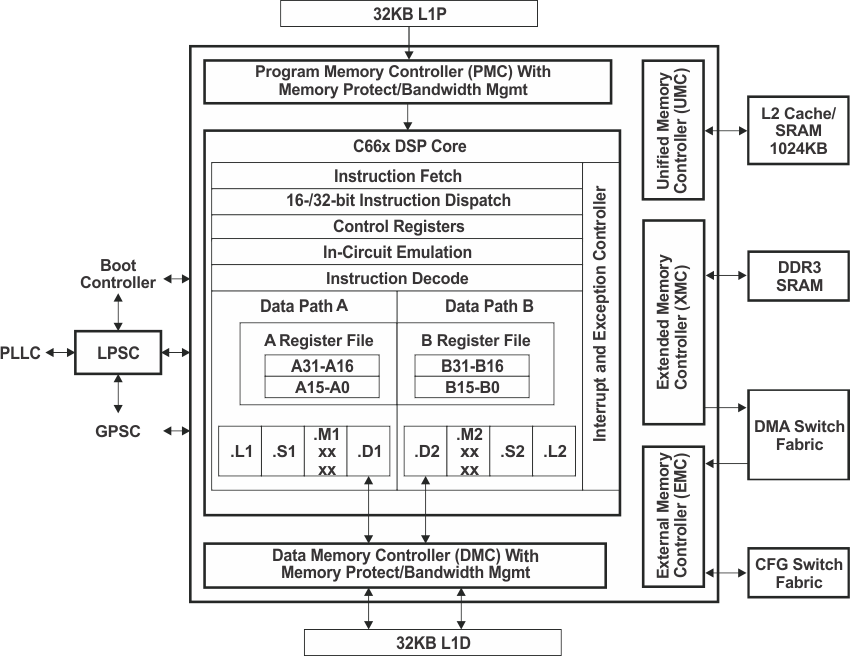
The C66x CorePac consists of several components:
- The C66x DSP and associated C66x CorePac core
- Level-one and level-two memories (L1P, L1D, L2)
- Data Trace Formatter (DTF)
- Embedded Trace Buffer (ETB)
- Interrupt Controller
- Power-down controller
- External Memory Controller
- Extended Memory Controller
- A dedicated power/sleep controller (LPSC)
The C66x CorePac also provides support for memory protection, bandwidth management (for resources local to the C66x CorePac) and address extension. Figure 6-1 shows a block diagram of the C66x CorePac.
 Figure 6-1 C66x CorePac Block Diagram
For more detailed information on the TMS320C66x CorePac on the C6654 device, see the C66x CorePac User's Guide (SPRUGW0).
6.1 Memory Architecture
The C66x CorePac in the device contains a 1024KB level-2 memory (L2), a 32KB level-1 program memory (L1P), and a 32KB level-1 data memory (L1D). The C6654 devices also contain a 1024KB multicore shared memory (MSM). All memory on the C6654 has a unique location in the memory map (see Table 3-2).
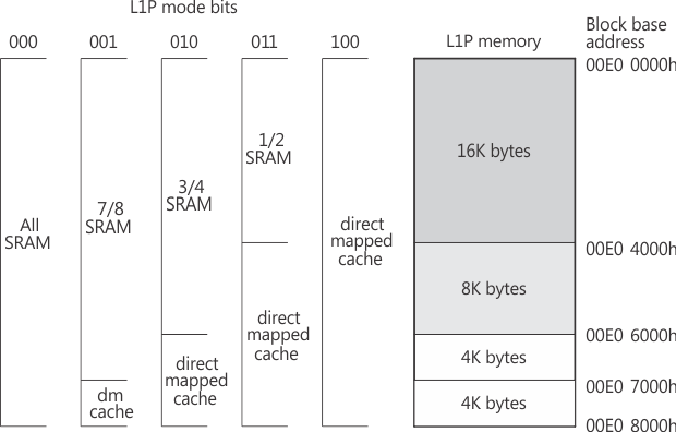
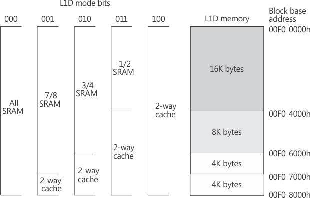
After device reset, L1P and L1D cache are configured as all cache, by default. The L1P and L1D cache can be reconfigured via software through the L1PMODE field of the L1P Configuration Register (L1PCFG) and the L1DMODE field of the L1D Configuration Register (L1DCFG) of the C66x CorePac. L1D is a two-way set-associative cache, while L1P is a direct-mapped cache.
The on-chip bootloader changes the reset configuration for L1P and L1D. For more information, see the Bootloader for the C66x DSP User's Guide (SPRUGY5).
For more information on the operation L1 and L2 caches, see the C66x DSP Cache User's Guide (SPRUGY8).
6.1.1 L1P Memory
The L1P memory configuration for the C6654 device is as follows:
- 32K bytes with no wait states
Figure 6-2 shows the available SRAM/cache configurations for L1P.
 Figure 6-2 L1P Memory Configurations
6.1.2 L1D Memory
The L1D memory configuration for the C6654 device is as follows:
- 32K bytes with no wait states
Figure 6-3 shows the available SRAM/cache configurations for L1D.
 Figure 6-3 L1D Memory Configurations
6.1.3 L2 Memory
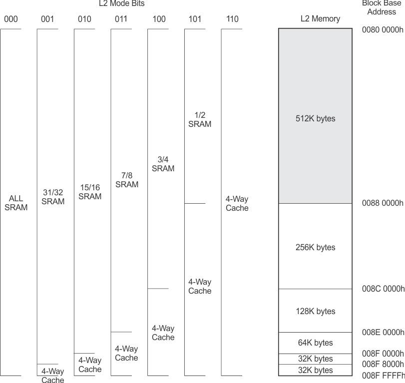
The L2 memory configuration for the C6654 device is as follows:
- Total memory is 1024KB
- Each core contains 1024KB of memory
- Local starting address for each core is 0080 0000h
L2 memory can be configured as all SRAM, all 4-way set-associative cache, or a mix of the two. The amount of L2 memory that is configured as cache is controlled through the L2MODE field of the L2 Configuration Register (L2CFG) of the C66x CorePac. Figure 6-4 shows the available SRAM/cache configurations for L2. By default, L2 is configured as all SRAM after device reset.
 Figure 6-4 L2 Memory Configurations
Global addresses are accessible to all masters in the system. In addition, local memory can be accessed directly by the associated processor through aliased addresses, where the eight MSBs are masked to zero. The aliasing is handled within the C66x CorePac and allows for common code to be run unmodified on multiple cores. For example, address location 0x10800000 is the global base address for C66x CorePac Core 0's L2 memory. C66x CorePac Core 0 can access this location by either using 0x10800000 or 0x00800000. Any other master on the device must use 0x10800000 only. Conversely, 0x00800000 can by used by any of the cores as their own L2 base addresses.
For C66x CorePac Core 0, address 0x00800000 is equivalent to 0x10800000. Local addresses should be used only for shared code or data, allowing a single image to be included in memory. Any code/data targeted to a specific core, or a memory region allocated during run-time by a particular core should always use the global address only.
6.1.4 MSM Controller
The MSM configuration for the device is as follows:
- Allows extension of external addresses from 2GB to up to 8GB
- Has built in memory protection features
For more details on external memory address extension and memory protection features, see the Multicore Shared Memory Controller (MSMC) for KeyStone Devices User's Guide (SPRUGW7).
6.1.5 L3 Memory
The L3 ROM on the device is 128KB. The ROM contains software used to boot the device. There is no requirement to block accesses from this portion to the ROM.
6.2 Memory Protection
Memory protection allows an operating system to define who or what is authorized to access L1D, L1P, and L2 memory. To accomplish this, the L1D, L1P, and L2 memories are divided into pages. There are 16 pages of L1P (2KB each), 16 pages of L1D (2KB each), and 32 pages of L2 (16KB each). The L1D, L1P, and L2 memory controllers in the C66x CorePac are equipped with a set of registers that specify the permissions for each memory page.
Each page may be assigned with fully orthogonal user and supervisor read, write, and execute permissions. In addition, a page may be marked as either (or both) locally accessible or globally accessible. A local access is a direct DSP access to L1D, L1P, and L2, while a global access is initiated by a DMA (either IDMA or the EDMA3) or by other system masters. Note that EDMA or IDMA transfers programmed by the DSP count as global accesses.
The DSP and each of the system masters on the device are all assigned a privilege ID. It is possible to specify whether memory pages are locally or globally accessible.
The AIDx and LOCAL bits of the memory protection page attribute registers specify the memory page protection scheme, see Table 6-1.
Table 6-1 Available Memory Page Protection Schemes
| AIDx BIT | LOCAL BIT | DESCRIPTION |
|---|---|---|
| 0 | 0 | No access to memory page is permitted. |
| 0 | 1 | Only direct access by DSP is permitted. |
| 1 | 0 | Only accesses by system masters and IDMA are permitted (includes EDMA and IDMA accesses initiated by the DSP). |
| 1 | 1 | All accesses permitted. |
Faults are handled by software in an interrupt (or an exception, programmable within the C66x CorePac interrupt controller) service routine. A DSP or DMA access to a page without the proper permissions will:
- Block the access — reads return 0, writes are ignored
- Capture the initiator in a status register — ID, address, and access type are stored
- Signal event to DSP interrupt controller
The software is responsible for taking corrective action to respond to the event and resetting the error status in the memory controller. For more information on memory protection for L1D, L1P, and L2, see the C66x CorePac User's Guide (SPRUGW0).
6.3 Bandwidth Management
When multiple requestors contend for a single C66x CorePac resource, the conflict is resolved by granting access to the highest priority requestor. The following four resources are managed by the Bandwidth Management control hardware:
- Level 1 Program (L1P) SRAM/Cache
- Level 1 Data (L1D) SRAM/Cache
- Level 2 (L2) SRAM/Cache
- Memory-mapped registers configuration bus
The priority level for operations initiated within the C66x CorePac are declared through registers in the C66x CorePac. These operations are:
- DSP-initiated transfers
- User-programmed cache coherency operations
- IDMA-initiated transfers
The priority level for operations initiated outside the C66x CorePac by system peripherals is declared through the Priority Allocation Register (PRI_ALLOC), see Section 5.4 for more details. System peripherals with no fields in the PRI_ALLOC have their own registers to program their priorities.
More information on the bandwidth management features of the C66x CorePac can be found in the C66x CorePac User's Guide (SPRUGW0).
6.4 Power-Down Control
The C66x CorePac supports the ability to power down various parts of the C66x CorePac. The power down controller (PDC) of the C66x CorePac can be used to power down L1P, the cache control hardware, the DSP, and the entire C66x CorePac. These power-down features can be used to design systems for lower overall system power requirements.
NOTE
The C6654 does not support power-down modes for the L2 memory at this time.
More information on the power-down features of the C66x CorePac can be found in the C66x CorePac User's Guide (SPRUGW0).
6.5 C66x CorePac Revision
The version and revision of the C66x CorePac can be read from the CorePac Revision ID Register (MM_REVID) located at address 0181 2000h. The MM_REVID register is shown in Figure 6-5 and described in Table 6-2. The C66x CorePac revision is dependent on the silicon revision being used.
| 31 | 16 | 15 | 0 |
| VERSION | REVISION |
| R-n | R-n |
| Legend: R = Read; -n = value after reset |
Table 6-2 CorePac Revision ID Register (MM_REVID) Field Descriptions
| Bit | Field | Description |
|---|---|---|
| 31-16 | VERSION | Version of the C66x CorePac implemented on the device. |
| 15-0 | REVISION | Revision of the C66x CorePac version implemented on the device. |
6.6 C66x CorePac Register Descriptions
See the C66x CorePac Reference Guide (SPRUGW0) for register offsets and definitions.