ZHCSDR5B March 2012 – April 2015 TMS320C6654
PRODUCTION DATA.
- 1 C6654 特性和描述
- 2 修订历史记录
-
3 Device Overview
- 3.1 Device Characteristics
- 3.2 DSP Core Description
- 3.3 Memory Map Summary
- 3.4 Boot Sequence
- 3.5
Boot Modes Supported and PLL Settings
- 3.5.1 Boot Device Field
- 3.5.2 Device Configuration Field
- 3.5.3
Boot Parameter Table
- 3.5.3.1 Sleep / XIP Mode Parameter Table
- 3.5.3.2 SRIO Mode Boot Parameter Table
- 3.5.3.3 Ethernet Mode Boot Parameter Table
- 3.5.3.4 NAND Mode Boot Parameter Table
- 3.5.3.5 PCIE Mode Boot Parameter Table
- 3.5.3.6 I2C Mode Boot Parameter Table
- 3.5.3.7 SPI Mode Boot Parameter Table
- 3.5.3.8 Hyperlink Mode Boot Parameter Table
- 3.5.3.9 UART Mode Boot Parameter Table
- 3.6 PLL Boot Configuration Settings
- 3.7 Second-Level Bootloaders
- 3.8 Terminals
- 3.9 Terminal Functions
-
4 Device Configuration
- 4.1 Device Configuration at Device Reset
- 4.2 Peripheral Selection After Device Reset
- 4.3
Device State Control Registers
- 4.3.1 Device Status Register
- 4.3.2 Device Configuration Register
- 4.3.3 JTAG ID (JTAGID) Register Description
- 4.3.4 Kicker Mechanism (KICK0 and KICK1) Register
- 4.3.5 LRESETNMI PIN Status (LRSTNMIPINSTAT) Register
- 4.3.6 LRESETNMI PIN Status Clear (LRSTNMIPINSTAT_CLR) Register
- 4.3.7 Reset Status (RESET_STAT) Register
- 4.3.8 Reset Status Clear (RESET_STAT_CLR) Register
- 4.3.9 Boot Complete (BOOTCOMPLETE) Register
- 4.3.10 Power State Control (PWRSTATECTL) Register
- 4.3.11 NMI Event Generation to CorePac (NMIGRx) Register
- 4.3.12 IPC Generation (IPCGRx) Registers
- 4.3.13 IPC Acknowledgement (IPCARx) Registers
- 4.3.14 IPC Generation Host (IPCGRH) Register
- 4.3.15 IPC Acknowledgement Host (IPCARH) Register
- 4.3.16 Timer Input Selection Register (TINPSEL)
- 4.3.17 Timer Output Selection Register (TOUTPSEL)
- 4.3.18 Reset Mux (RSTMUXx) Register
- 4.3.19 Device Speed (DEVSPEED) Register
- 4.3.20 Pin Control 0 (PIN_CONTROL_0) Register
- 4.3.21 Pin Control 1 (PIN_CONTROL_1) Register
- 4.3.22 uPP Clock Source (UPP_CLOCK) Register
- 4.4 Pullup/Pulldown Resistors
- 5 System Interconnect
- 6 C66x CorePac
- 7 Device Operating Conditions
-
8 Peripheral Information and Electrical Specifications
- 8.1 Recommended Clock and Control Signal Transition Behavior
- 8.2 Power Supplies
- 8.3 Power Sleep Controller (PSC)
- 8.4 Reset Controller
- 8.5
Main PLL and PLL Controller
- 8.5.1 Main PLL Controller Device-Specific Information
- 8.5.2
PLL Controller Memory Map
- 8.5.2.1 PLL Secondary Control Register (SECCTL)
- 8.5.2.2 PLL Controller Divider Register (PLLDIV2, PLLDIV5, PLLDIV8)
- 8.5.2.3 PLL Controller Clock Align Control Register (ALNCTL)
- 8.5.2.4 PLLDIV Divider Ratio Change Status Register (DCHANGE)
- 8.5.2.5 SYSCLK Status Register (SYSTAT)
- 8.5.2.6 Reset Type Status Register (RSTYPE)
- 8.5.2.7 Reset Control Register (RSTCTRL)
- 8.5.2.8 Reset Configuration Register (RSTCFG)
- 8.5.2.9 Reset Isolation Register (RSISO)
- 8.5.3 Main PLL Control Register
- 8.5.4 Main PLL and PLL Controller Initialization Sequence
- 8.5.5 Main PLL Controller/PCIe Clock Input Electrical Data/Timing
- 8.6 DDR3 PLL
- 8.7 Enhanced Direct Memory Access (EDMA3) Controller
- 8.8 Interrupts
- 8.9 Memory Protection Unit (MPU)
- 8.10 DDR3 Memory Controller
- 8.11 I2C Peripheral
- 8.12 SPI Peripheral
- 8.13 UART Peripheral
- 8.14 PCIe Peripheral
- 8.15 EMIF16 Peripheral
- 8.16 Ethernet Media Access Controller (EMAC)
- 8.17 Management Data Input/Output (MDIO)
- 8.18 Timers
- 8.19 General-Purpose Input/Output (GPIO)
- 8.20 Semaphore2
- 8.21 Multichannel Buffered Serial Port (McBSP)
- 8.22 Universal Parallel Port (uPP)
- 8.23 Emulation Features and Capability
- 9 Device and Documentation Support
- 10Mechanical Data
5 System Interconnect
On the C6654 device, the C66x CorePac, the EDMA3 transfer controller, and the system peripherals are interconnected through the TeraNet, which is a non-blocking switch fabric enabling fast and contention-free internal data movement. The TeraNet allows for low-latency, concurrent data transfers between master peripherals and slave peripherals. The TeraNet also allows for seamless arbitration between the system masters when accessing system slaves.
5.1 Internal Buses and Switch Fabrics
Two types of buses exist in the device: data buses and configuration buses. Some peripherals have both a data bus and a configuration bus interface, while others have only one type of interface. Further, the bus interface width and speed varies from peripheral to peripheral. Configuration buses are mainly used to access the register space of a peripheral and the data buses are used mainly for data transfers.
The C66x CorePac, the EDMA3 traffic controller, and the various system peripherals can be classified into two categories: masters and slaves. Masters are capable of initiating read and write transfers in the system and do not rely on the EDMA3 for their data transfers. Slaves, on the other hand, rely on the masters to perform transfers to and from them. Examples of masters include the EDMA3 traffic controller and PCI Express. Examples of slaves include the SPI, UART, and I2C.
The masters and slaves in the device are communicating through the TeraNet (switch fabric). The device contains two switch fabrics. The data switch fabric (data TeraNet) and the configuration switch fabric (configuration TeraNet). The data TeraNet, is a high-throughput interconnect mainly used to move data across the system. The data TeraNet connects masters to slaves via data buses. The configuration TeraNet, is mainly used to access peripheral registers. The configuration TeraNet connects masters to slaves via configuration buses. Note that the data TeraNet also connects to the configuration TeraNet. For more details see Section 5.2.
5.2 Switch Fabric Connections Matrix
The tables below list the master and slave end point connections.
Intersecting cells may contain one of the following:
- Y — There is a connection between this master and that slave.
- - — There is NO connection between this master and that slave.
- n — A numeric value indicates that the path between this master and that slave goes through bridge n.
Table 5-1 Switch Fabric Connection Matrix Section 1
| MASTERS | SLAVES | |||||||||||||||||
|---|---|---|---|---|---|---|---|---|---|---|---|---|---|---|---|---|---|---|
| CorePac0_SDMA | PCIe0_Slave | Boot_ROM | SPI | EMIF16 | Mcbsp0_FIFO_Data | Mcbsp1_FIFO_Data | QM_Slave | MSMC_SES | STM | TETB_D | TETB0 | EDMA3CC | EDMA3TC(0-3) | Semaphore | QM__CFG | Tracer | Timer | |
| EDMA3CC_TC0_RD | Y | Y | Y | Y | Y | - | - | - | Y | - | 1 | - | 1 | 1 | 1 | 1 | 1 | 1, 4 |
| EDMA3CC_TC0_WR | Y | Y | - | Y | Y | - | - | - | Y | 1 | - | - | 1 | 1 | 1 | 1 | 1 | 1, 4 |
| EDMA3CC_TC1_RD | Y | Y | Y | Y | Y | 2, 4 | 2, 4 | - | Y | - | - | 2 | 2 | 2 | - | - | - | - |
| EDMA3CC_TC1_WR | Y | Y | - | Y | Y | 2, 4 | 2, 4 | - | Y | - | - | - | 2 | 2 | - | - | - | - |
| EDMA3CC_TC2_RD | Y | Y | Y | Y | Y | 1, 4 | 1, 4 | - | Y | - | 1 | - | 1 | 1 | 1 | 1 | 1 | 1, 4 |
| EDMA3CC_TC2_WR | Y | Y | - | Y | Y | 1, 4 | 1, 4 | - | Y | - | - | - | 1 | 1 | 1 | 1 | 1 | 1, 4 |
| EDMA3CC_TC3_RD | Y | Y | Y | Y | Y | - | - | 2 | Y | - | - | - | 2 | 2 | - | - | - | - |
| EDMA3CC_TC3_WR | Y | Y | - | Y | Y | - | - | 2 | Y | 2 | - | - | 2 | 2 | - | - | - | - |
| PCIe_Master | Y | - | - | Y | Y | 1, 4 | 1, 4 | 1 | Y | 1 | 1 | 1 | 1 | 1 | 1 | 1 | 1 | 1, 4 |
| EMAC | 3 | - | - | - | - | - | - | - | 3 | - | - | - | - | - | - | - | - | - |
| MSMC_Data_Master | Y | Y | Y | Y | Y | 1, 4 | 1, 4 | 1 | - | 1 | - | - | - | - | - | - | - | - |
| QM Packet DMA | Y | - | - | - | - | - | - | 1 | Y | - | - | - | - | - | - | - | - | - |
| QM Second | Y | - | Y | Y | Y | - | - | 1 | Y | - | - | - | - | - | - | - | - | - |
| DAP_Master | Y | Y | Y | Y | Y | 1, 4 | 1, 4 | 1 | Y | 1 | 1 | 1 | 1 | 1 | 1 | 1 | 1 | 1, 4 |
| CorePac0_CFG | - | - | - | - | - | - | - | - | - | - | - | - | - | Y | - | - | - | - |
| Tracer_Master | - | - | - | - | - | - | - | - | - | 1 | Y | Y | Y | Y | Y | Y | Y | 4 |
| uPP | 3 | - | - | - | - | - | - | - | 3 | - | - | - | - | - | - | - | ||
Table 5-2 Switch Fabric Connection Matrix Section 2
| MASTERS | SLAVES | |||||||||||||||||
|---|---|---|---|---|---|---|---|---|---|---|---|---|---|---|---|---|---|---|
| GPIO | I2C | SEC_CTL | SEC_KEY_MGR | Efuse | Boot_CFG | PSC | PLL | CIC | MPU0-3 | MPU4 | Debug_SS_CFG | SmartReflex | UART_CFG (0-1) | McBSP_CFG(0-1) | McBSP_FIFO_CFG(0-1) | EMAC_CFG | UPP_CFG | |
| EDMA3CC_TC0_RD | 1, 4 | 1, 4 | 1, 4 | 1, 4 | - | 1, 4 | 1, 4 | 1, 4 | 1, 4 | 1 | 1, 4 | - | - | 1, 4 | 1, 4 | 1, 4 | 1, 4 | 1 |
| EDMA3CC_TC0_WR | 1, 4 | 1, 4 | 1, 4 | 1, 4 | - | 1, 4 | 1, 4 | 1, 4 | 1, 4 | 1 | 1, 4 | - | - | 1, 4 | 1, 4 | 1, 4 | 1, 4 | 1 |
| EDMA3CC_TC1_RD | - | - | - | - | - | - | - | - | - | - | - | - | - | - | - | - | - | - |
| EDMA3CC_TC1_WR | - | - | - | - | - | - | - | - | - | - | - | - | - | - | - | - | - | - |
| EDMA3CC_TC2_RD | 1, 4 | 1, 4 | 1, 4 | 1, 4 | - | 1, 4 | 1, 4 | 1, 4 | 1, 4 | 1 | 1, 4 | - | - | 1, 4 | 1, 4 | 1, 4 | 1, 4 | 1 |
| EDMA3CC_TC2_WR | 1, 4 | 1, 4 | 1, 4 | 1, 4 | - | 1, 4 | 1, 4 | 1, 4 | 1, 4 | 1 | 1, 4 | - | - | 1, 4 | 1, 4 | 1, 4 | 1, 4 | 1 |
| EDMA3CC_TC3_RD | - | - | - | - | - | - | - | - | - | - | - | - | - | - | - | - | - | - |
| EDMA3CC_TC3_WR | - | - | - | - | - | - | - | - | - | - | - | - | - | - | - | - | - | - |
| PCIe_Master | 1, 4 | 1, 4 | 1, 4 | 1, 4 | - | 1, 4 | 1, 4 | 1, 4 | 1, 4 | 1 | 1, 4 | 1, 4 | 1, 4 | 1, 4 | 1, 4 | 1, 4 | 1, 4 | 1 |
| EMAC | - | - | - | - | - | - | - | - | - | - | - | - | - | - | - | - | - | - |
| MSMC_Data_Master | - | - | - | - | - | - | - | - | - | - | - | - | - | - | - | - | - | |
| QM Packet DMA | - | - | - | - | - | - | - | - | - | - | - | - | - | - | - | - | - | - |
| QM Second | - | - | - | - | - | - | - | - | - | - | - | - | - | - | - | - | - | - |
| DAP_Master | 1, 4 | 1, 4 | 1, 4 | 1, 4 | 1, 4 | 1, 4 | 1, 4 | 1, 4 | 1, 4 | 1 | 1, 4 | 1, 4 | 1, 4 | 1, 4 | 1, 4 | 1, 4 | 1, 4 | 1 |
| EDMA3CC | - | - | - | - | - | - | - | - | - | - | - | - | - | - | - | - | - | - |
| CorePac0_CFG | 4 | 4 | 4 | 4 | 4 | 4 | 4 | 4 | 4 | Y | 4 | 4 | 4 | 4 | 4 | 4 | 4 | Y |
| Tracer_Master | - | - | - | - | - | - | - | - | - | - | - | - | - | - | - | - | - | - |
| uPP | - | - | - | - | - | - | - | - | - | - | - | - | - | - | - | - | - | - |
5.3 TeraNet Switch Fabric Connections
The figures below show the connections between masters and slaves through various sections of the TeraNet.
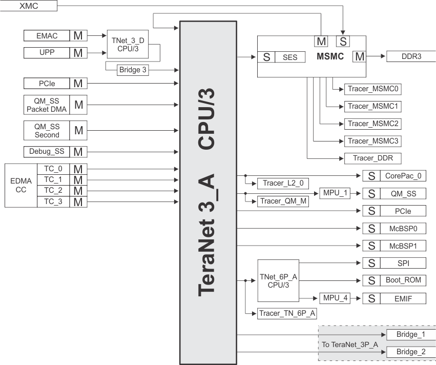 Figure 5-1 TeraNet 3A
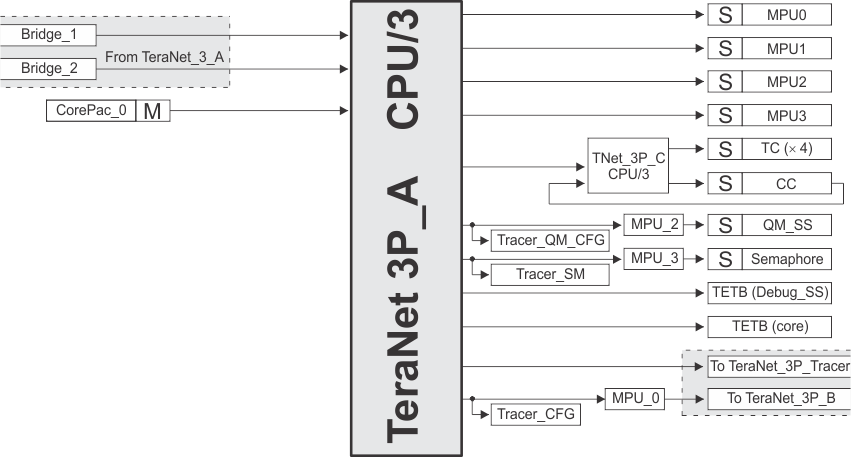 Figure 5-2 TeraNet 3P_A
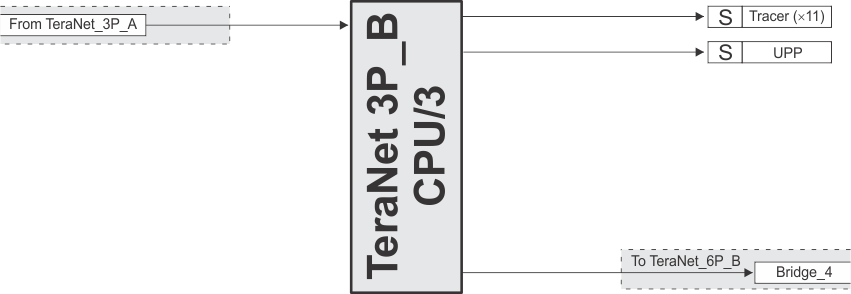 Figure 5-3 TeraNet 3P_B
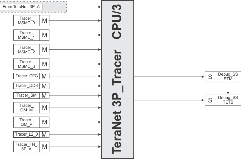 Figure 5-4 TeraNet 3P_Tracer
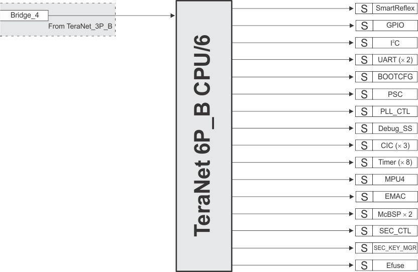 Figure 5-5 TeraNet 6P_B
5.4 Bus Priorities
The priority level of all master peripheral traffic is defined at the TeraNet boundary. User programmable priority registers allow software configuration of the data traffic through the TeraNet. Note that a lower number means higher priority - PRI = 000b = urgent, PRI = 111b = low.
Most master ports provide their priority directly and do not need a default priority setting. Examples include the CorePacs, whose priorities are set through software in the UMC control registers. All the packet-DMA-based peripherals also have internal registers to define the priority level of their initiated transactions.
Some masters do not have apriority allocation register of their own. For these masters, a priority allocation register is provided for them and described in the sections below. For all other modules, see the respective User Guides in Section 9.2 for programmable priority registers.
5.4.1 Packet DMA Priority Allocation (PKTDMA_PRI_ALLOC) Register
The packet DMA secondary port is one master port that does not have priority allocation register inside the IP. The priority level for transaction from this master port is described by PKTDMA_PRI_ALLOC register in Figure 5-6 and Table 5-3.
| 31 | 3 | 2 | 0 |
| Reserved | PKTDMA_PRI | ||||||||||||||
| R/W-00000000000000000000001000011 | RW-000 | ||||||||||||||
| LEGEND: R/W = Read/Write; R = Read only; -n = value after reset |
Table 5-3 Packet DMA Priority Allocation Register (PKTDMA_PRI_ALLOC) Field Descriptions
| Bit | Name | Description |
|---|---|---|
| 31-3 | Reserved | Reserved |
| 2-0 | PKTDMA_PRI | Control the priority level for the transactions from packet DMA master port, which access the external linking RAM. |
5.4.2 EMAC / uPP Priority Allocation (EMAC_UPP_PRI_ALLOC) Register
The EMAC and uPP are master ports that do not have priority allocation registers inside the IP. The priority level for transaction from these master ports is described by EMAC_UPP_PRI_ALLOC register in Figure 5-7 and Table 5-4.
| 31 | 27 | 26 | 24 | 23 | 19 | 18 | 16 | 15 | 11 | 10 | 8 | 7 | 3 | 2 | 0 |
| Reserved | EMAC_EPRI | Reserved | EMAC_PRI | Reserved | UPP_EPRI | Reserved | UPP_PRI |
| R-00000 | RW-110 | R-00000 | RW-111 | R-00000 | RW-110 | R-00000 | RW-111 |
| LEGEND: R/W = Read/Write; R = Read only; -n = value after reset |
Table 5-4 EMAC / uPP Priority Allocation Register (EMAC_UPP_PRI_ALLOC) Field Descriptions
| Bit | Name | Description |
|---|---|---|
| 31-27 | Reserved | Reserved |
| 26-24 | EMAC_EPRI | Control the maximum priority level for the transactions from EMAC master port. |
| 23-19 | Reserved | Reserved |
| 18-16 | EMAC_PRI | Control the priority level for the transactions from EMAC master port. |
| 15-11 | Reserved | Reserved |
| 10-8 | UPP_EPRI | Control the maximum priority level for the transactions from uPP master port. |
| 7-3 | Reserved | Reserved |
| 2-0 | UPP_PRI | Control the priority level for the transactions from uPP master port. |