ZHCSH87B September 2017 – February 2020 TMP461-SP
PRODUCTION DATA.
- 1 特性
- 2 应用
- 3 说明
- 4 修订历史记录
- 5 Pin Configuration and Functions
- 6 Specifications
-
7 Detailed Description
- 7.1 Overview
- 7.2 Functional Block Diagram
- 7.3 Feature Description
- 7.4 Device Functional Modes
- 7.5 Programming
- 7.6
Register Map
- 7.6.1
Register Information
- 7.6.1.1 Pointer Register
- 7.6.1.2 Local and Remote Temperature Registers
- 7.6.1.3 Status Register
- 7.6.1.4 Configuration Register
- 7.6.1.5 Conversion Rate Register
- 7.6.1.6 One-Shot Start Register
- 7.6.1.7 Channel Enable Register
- 7.6.1.8 Consecutive ALERT Register
- 7.6.1.9 η-Factor Correction Register
- 7.6.1.10 Remote Temperature Offset Register
- 7.6.1.11 Manufacturer Identification Register
- 7.6.1
Register Information
- 8 Application and Implementation
- 9 Power Supply Recommendations
- 10Layout
- 11器件和文档支持
- 12机械、封装和可订购信息
7.5.1.2 Bus Definitions
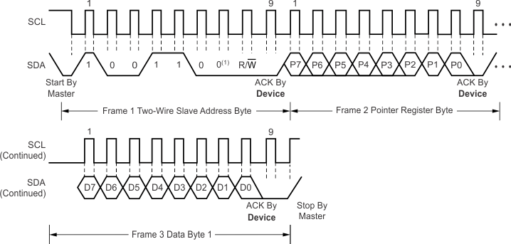
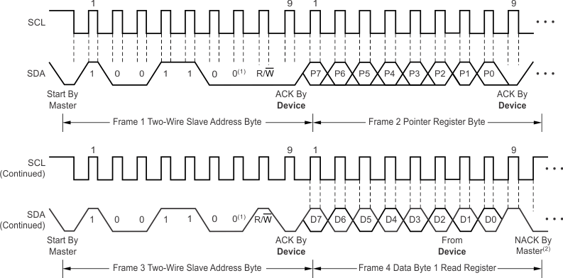
The TMP461-SP device is two-wire- and SMBus-compatible. Figure 15 and Figure 16 illustrate the timing for various operations on the TMP461-SP device. The bus definitions are as follows:
- Bus Idle: Both SDA and SCL lines remain high.
- Start Data Transfer:A change in the state of the SDA line (from high to low) when the SCL line is high defines a start condition. Each data transfer initiates with a start condition.
- Stop Data Transfer: A change in the state of the SDA line (from low to high) when the SCL line is high defines a stop condition. Each data transfer terminates with a repeated start or stop condition.
- Data Transfer:The number of data bytes transferred between a start and stop condition is not limited and is determined by the master device. The receiver acknowledges the data transfer.
- Acknowledge:Each receiving device, when addressed, is obliged to generate an acknowledge bit. A device that acknowledges must pull down the SDA line during the acknowledge clock pulse in such a way that the SDA line is stable low during the high period of the acknowledge clock pulse. Take setup and hold times into account. On a master receive, data transfer termination can be signaled by the master generating a not-acknowledge on the last byte that is transmitted by the slave.

1. Slave address 1001100 is shown.
Figure 15. Two-Wire Timing Diagram for Write Word Format 
1. Slave address 1001100 is shown.
2. The master must leave SDA high to terminate a single-byte read operation.
Figure 16. Two-Wire Timing Diagram for Single-Byte Read Format