ZHCSP20 September 2022 TLV61070A
PRODUCTION DATA
- 1 特性
- 2 应用
- 3 说明
- 4 Revision History
- 5 Pin Configuration and Functions
- 6 Specifications
- 7 Detailed Description
- 8 Application and Implementation
- 9 Device and Documentation Support
- 10Mechanical, Packaging, and Orderable Information
8.2.2.1 Setting the Output Voltage
The output voltage is set by an external resistor divider (R1, R2 in Figure 8-1). When the output voltage is regulated, the typical voltage at the FB pin is VREF. Thus, the resistor divider is determined by Equation 4.
Equation 4. 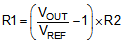
where
- VOUT is the regulated output voltage
- VREF is the internal reference voltage at the FB pin
For the best accuracy, keep R2 smaller than 100 kΩ to ensure the current flowing through R2 is at least 100 times larger than the FB pin leakage current. Changing R2 towards a lower value increases the immunity against noise injection. Changing the R2 towards a higher value reduces the quiescent current for achieving highest efficiency at low load currents.