SLVSLE3 May   2026 TLV4825

ADVANCE INFORMATION  

  1.   1
  2. Features
  3. Applications
  4. Description
  5. Pin Configuration and Functions
  6. Specifications
    1. 5.1 Absolute Maximum Ratings
    2. 5.2 ESD Ratings
    3. 5.3 Recommended Operating Conditions
    4. 5.4 Thermal Information for Single Channel
    5. 5.5 Thermal Information for Dual Channel
    6. 5.6 Thermal Information for Quad Channel
    7. 5.7 Electrical Characteristics
    8. 5.8 Typical Characteristics
  7. Detailed Description
    1. 6.1 Overview
    2. 6.2 Functional Block Diagram
    3. 6.3 Feature Description
      1. 6.3.1 Operating Voltage
      2. 6.3.2 Input Common-Mode Range
      3. 6.3.3 Output Range
      4. 6.3.4 Capacitive Load and Stability
      5. 6.3.5 Overload Recovery
      6. 6.3.6 Phase-Reversal Protection
      7. 6.3.7 Chopping Transients
      8. 6.3.8 EMI Rejection
      9. 6.3.9 Electrical Overstress
    4. 6.4 Device Functional Modes
  8. Application and Implementation
    1. 7.1 Application Information
      1. 7.1.1 Basic Noise Calculations
    2. 7.2 Typical Application
      1. 7.2.1 TLVx825 in Low-Side, Current Sensing Application
        1. 7.2.1.1 Design Requirements
        2. 7.2.1.2 Detailed Design Procedure
        3. 7.2.1.3 Application Curve
    3. 7.3 Power Supply Recommendations
    4. 7.4 Layout
      1. 7.4.1 Layout Guidelines
      2. 7.4.2 Layout Example
  9. Device and Documentation Support
    1. 8.1 Device Support
      1. 8.1.1 Development Support
        1. 8.1.1.1 PSpice® for TI
        2. 8.1.1.2 TINA-TI™ Simulation Software (Free Download)
    2. 8.2 Documentation Support
      1. 8.2.1 Related Documentation
    3. 8.3 Receiving Notification of Documentation Updates
    4. 8.4 Support Resources
    5. 8.5 Trademarks
    6. 8.6 Electrostatic Discharge Caution
    7. 8.7 Glossary
  10. Revision History
  11. 10Mechanical, Packaging, and Orderable Information
    1. 10.1 Mechanical Data
    2. 10.2 Tape and Reel Information

请参考 PDF 数据表获取器件具体的封装图。

机械数据 (封装 | 引脚)
  • D|14
散热焊盘机械数据 (封装 | 引脚)

Typical Characteristics

at TA = 25°C, VS = ±2.75V, VCM = VS / 2, and RL = 10kΩ (unless otherwise noted)

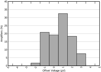
TLV825 TLV2825 TLV4825 Offset Voltage
            Distribution
VS = 5.5V VCM = VS / 2 TA = 25°C
N = 120 Mean = 0.03µV Sigma = 1.02µV
Figure 5-1 Offset Voltage Distribution
TLV825 TLV2825 TLV4825 Offset Voltage Distribution
VS = 5.5V VCM = VS / 2 TA = –40°C
N = 120 Mean = –0.64µV Sigma = 1.2µV
Figure 5-3 Offset Voltage Distribution
TLV825 TLV2825 TLV4825 Input Bias
            Current Distribution
VS = 5.5V VCM = VS / 2 TA = 25°C
N = 120 Mean = 35.9pA Sigma = 16.1pA
Figure 5-5 Input Bias Current Distribution
TLV825 TLV2825 TLV4825 Input Bias
            Current Distribution
VS = 5.5V VCM = VS / 2 TA = 125°C
N = 120 Mean = 35.9pA Sigma = 16.1pA
Figure 5-7 Input Bias Current Distribution
TLV825 TLV2825 TLV4825 Input Bias
            Current Distribution
VS = 1.8V VCM = VS / 2 TA = 25°C
N = 120 Mean = 36.7pA Sigma = 16.3pA
Figure 5-9 Input Bias Current Distribution
TLV825 TLV2825 TLV4825 Input Bias Current Distribution
VS = 1.8V VCM = VS / 2 TA = 125°C
N = 120 Mean = 34.1pA Sigma = 16.2pA
Figure 5-11 Input Bias Current Distribution
TLV825 TLV2825 TLV4825 Offset Voltage
            vs Common-Mode VoltageFigure 5-13 Offset Voltage vs Common-Mode Voltage
TLV825 TLV2825 TLV4825 Offset Voltage
            vs Supply VoltageFigure 5-15 Offset Voltage vs Supply Voltage
TLV825 TLV2825 TLV4825 Input Bias
            Current and Offset Current vs TemperatureFigure 5-17 Input Bias Current and Offset Current vs Temperature
TLV825 TLV2825 TLV4825 Closed-Loop
            Gain vs FrequencyFigure 5-19 Closed-Loop Gain vs Frequency
TLV825 TLV2825 TLV4825 Output Voltage
            Swing vs Output Current (Sinking)Figure 5-21 Output Voltage Swing vs
Output Current (Sinking)
TLV825 TLV2825 TLV4825 Output Voltage Swing vs Output
            Current (Sinking)
 VS = 1.8V
Figure 5-23 Output Voltage Swing vs
Output Current (Sinking)
TLV825 TLV2825 TLV4825 CMRR vs
            TemperatureFigure 5-25 CMRR vs Temperature
TLV825 TLV2825 TLV4825 0.1Hz to 10Hz
            Voltage NoiseFigure 5-27 0.1Hz to 10Hz Voltage Noise
TLV825 TLV2825 TLV4825 Phase Margin vs
            Cap Load Figure 5-29 Phase Margin vs Cap Load
TLV825 TLV2825 TLV4825 THD+N vs Output
            Amplitude
 f = 1kHz
Figure 5-31 THD+N vs Output Amplitude
TLV825 TLV2825 TLV4825 Quiescent
            Current vs TemperatureFigure 5-33 Quiescent Current vs Temperature
TLV825 TLV2825 TLV4825 Open-Loop
            Output Impedance vs FrequencyFigure 5-35 Open-Loop Output Impedance vs Frequency
TLV825 TLV2825 TLV4825 Small-Signal
            Overshoot vs Capacitive Load
Gain = 1, 10mV step
Figure 5-37 Small-Signal Overshoot vs
Capacitive Load
TLV825 TLV2825 TLV4825 Positive
            Overload RecoveryFigure 5-39 Positive Overload Recovery
TLV825 TLV2825 TLV4825 Small-Signal
            Step Response
Gain = 1, 10mV step
Figure 5-41 Small-Signal Step Response
TLV825 TLV2825 TLV4825 Large-Signal
            Step Response
Gain = 1, 4V step
Figure 5-43 Large-Signal Step Response
TLV825 TLV2825 TLV4825 Large-Signal
            Step Response
Gain = –1, 4V step
Figure 5-45 Large-Signal Step Response
TLV825 TLV2825 TLV4825 Maximum Output
            Voltage vs FrequencyFigure 5-47 Maximum Output Voltage vs Frequency
TLV825 TLV2825 TLV4825 Channel
            SeparationFigure 5-49 Channel Separation
TLV825 TLV2825 TLV4825 Offset Voltage
            Distribution
VS = 5.5V VCM = VS / 2 TA = 125°C
N = 120 Mean = 1.17µV Sigma = 1.22µV
Figure 5-2 Offset Voltage Distribution
TLV825 TLV2825 TLV4825 Offset Voltage
            Drift
VS = 5.5V VCM = VS / 2 N = 120
Mean = 0.013µV/°C Sigma = 0.007µV/°C
Figure 5-4 Offset Voltage Drift
TLV825 TLV2825 TLV4825 Input Offset
            Current Distribution
VS = 5.5V VCM = VS / 2 TA = 25°C
N = 120 Mean = 71.7pA Sigma = 32.1pA
Figure 5-6 Input Offset Current Distribution
TLV825 TLV2825 TLV4825 Input Offset Current Distribution
VS = 5.5V VCM = VS / 2 TA = 125°C
N = 120 Mean = 31.5pA Sigma = 15.7pA
Figure 5-8 Input Offset Current Distribution
TLV825 TLV2825 TLV4825 Input Offset Current Distribution
VS = 1.8V VCM = VS / 2 TA = 25°C
N = 120 Mean = 73.1pA Sigma = 32.4pA
Figure 5-10 Input Offset Current Distribution
TLV825 TLV2825 TLV4825 Input Offset Current Distribution
VS = 1.8V VCM = VS / 2 TA = 125°C
N = 120 Mean = 72pA Sigma = 32.4pA
Figure 5-12 Input Offset Current Distribution
TLV825 TLV2825 TLV4825 Offset Voltage
            vs TemperatureFigure 5-14 Offset Voltage vs Temperature
TLV825 TLV2825 TLV4825 Input Bias Current vs Common-Mode
            VoltageFigure 5-16 Input Bias Current vs Common-Mode Voltage
TLV825 TLV2825 TLV4825 Open-Loop Gain
            and Phase vs FrequencyFigure 5-18 Open-Loop Gain and Phase vs Frequency
TLV825 TLV2825 TLV4825 Output Voltage
            Swing vs Output Current (Sourcing)Figure 5-20 Output Voltage Swing vs
Output Current (Sourcing)
TLV825 TLV2825 TLV4825 Output Voltage Swing vs Output
            Current (Sourcing)
 VS = 1.8V
Figure 5-22 Output Voltage Swing vs
Output Current (Sourcing)
TLV825 TLV2825 TLV4825 CMRR and PSRR
            vs FrequencyFigure 5-24 CMRR and PSRR vs Frequency
TLV825 TLV2825 TLV4825 PSRR vs
            TemperatureFigure 5-26 PSRR vs Temperature
TLV825 TLV2825 TLV4825 Input Voltage
            Noise Spectral Density vs FrequencyFigure 5-28 Input Voltage Noise Spectral Density vs Frequency
TLV825 TLV2825 TLV4825 THD+N vs
            Frequency
 VOUT = 1VRMS
Figure 5-30 THD+N vs Frequency
TLV825 TLV2825 TLV4825 Quiescent
            Current vs Supply VoltageFigure 5-32 Quiescent Current vs Supply Voltage
TLV825 TLV2825 TLV4825 Open-Loop Gain
            vs TemperatureFigure 5-34 Open-Loop Gain vs Temperature
TLV825 TLV2825 TLV4825 Small-Signal
            Overshoot vs Capacitive Load
Gain = –1, 10mV step
Figure 5-36 Small-Signal Overshoot vs
Capacitive Load
TLV825 TLV2825 TLV4825 No Phase
            ReversalFigure 5-38 No Phase Reversal
TLV825 TLV2825 TLV4825 Negative
            Overload RecoveryFigure 5-40 Negative Overload Recovery
TLV825 TLV2825 TLV4825 Small-Signal
            Step Response
Gain = –1, 10mV step
Figure 5-42 Small-Signal Step Response
TLV825 TLV2825 TLV4825 Output Settling
            to Final Value
Gain = 1, 4V step
Figure 5-44 Output Settling to Final Value
TLV825 TLV2825 TLV4825 Short-Circuit
            Current vs TemperatureFigure 5-46 Short-Circuit Current vs Temperature
TLV825 TLV2825 TLV4825 EMIRR vs
            FrequencyFigure 5-48 EMIRR vs Frequency