ZHCSGU7 October   2017 TLV3544-Q1

PRODUCTION DATA.  

  1. 特性
  2. 应用
  3. 说明
  4. 修订历史记录
  5. Pin Configuration and Functions
  6. Specifications
    1. 6.1 Absolute Maximum Ratings
    2. 6.2 ESD Ratings
    3. 6.3 Recommended Operating Conditions
    4. 6.4 Thermal Information: TLV3544-Q1
    5. 6.5 Electrical Characteristics: VS = 2.7 V to 5.5 V Single-Supply
    6. 6.6 Typical Characteristics
  7. Detailed Description
    1. 7.1 Overview
    2. 7.2 Functional Block Diagram
    3. 7.3 Feature Description
      1. 7.3.1 TLV3544-Q1 Comparison
      2. 7.3.2 Operating Voltage
      3. 7.3.3 Rail-to-Rail Input
      4. 7.3.4 Rail-to-Rail Output
      5. 7.3.5 Output Drive
      6. 7.3.6 Video
      7. 7.3.7 Driving Analog-to-Digital converters
      8. 7.3.8 Capacitive Load and Stability
      9. 7.3.9 Wideband Transimpedance Amplifier
    4. 7.4 Device Functional Modes
  8. Application and Implementation
    1. 8.1 Application Information
    2. 8.2 Typical Application
      1. 8.2.1 Design Requirements
      2. 8.2.2 Detailed Design Procedure
        1. 8.2.2.1 Optimizing the Transimpedance Circuit
      3. 8.2.3 Application Curve
  9. Power Supply Recommendations
  10. 10Layout
    1. 10.1 Layout Guidelines
    2. 10.2 Layout Example
    3. 10.3 Power Dissipation
  11. 11器件和文档支持
    1. 11.1 文档支持
    2. 11.2 接收文档更新通知
    3. 11.3 社区资源
    4. 11.4 商标
    5. 11.5 静电放电警告
    6. 11.6 Glossary
  12. 12机械、封装和可订购信息

封装选项

机械数据 (封装 | 引脚)
散热焊盘机械数据 (封装 | 引脚)
订购信息

Pin Configuration and Functions

PW Package
14-Pin TSSOP
Top View
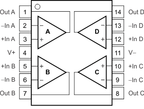
TLV3544-Q1 po_tssop_soic14_bos233.gif

Pin Functions

PIN I/O DESCRIPTION
NAME NO.
–In A 2 I Inverting input, channel A
+In A 3 I Noninverting input, channel A
–In B 6 I Inverting input, channel B
+In B 5 I Noninverting input, channel B
–In C 9 I Inverting input, channel C
+In C 10 I Noninverting input, channel C
–In D 13 I Inverting input, channel D
+In D 12 I Noninverting input, channel D
Out A 1 O Output, channel A
Out B 7 O Output, channel B
Out C 8 O Output, channel C
Out D 14 O Output, channel D
V– 11 Negative (lowest) supply
V+ 4 Positive (highest) supply