ZHCSAX3B March 2013 – May 2014 TLC5973
PRODUCTION DATA.
- 1 特性
- 2 应用范围
- 3 说明
- 4 修订历史记录
- 5 Pin Configuration and Functions
- 6 Specifications
- 7 Parameter Measurement Information
- 8 Detailed Description
- 9 Applications and Implementation
- 10Power Supply Recommendations
- 11Layout
- 12器件和文档支持
- 13机械封装和可订购信息
9 Applications and Implementation
9.1 Application Information
The device is a constant sink current LED driver. This device is typically used to minimize wiring cost in applications and also provides no restrictions of cascading multiple devices in series. Furthermore, the device maximum data transfer rate is 3 Mbps and can contribute high-frequency display data change rates. The following design procedures can be used to maximize application design with minimal wiring cost. The device is also a good choice for higher VCC power-supply voltage applications because of the internal shunt regulator included in the device.
9.2 Typical Applications
9.2.1 No Internal Shunt Regulator Mode 1
This application does not use the shunt regulator. However, the device VCC and LED lamp anode voltage can be supplied from the same power supply because only one LED lamp is connected in series.
 Figure 22. No Internal Shunt Regulator Mode 1 Typical Application Circuit
9.2.1.1 Design Requirements
Table 4. Design Parameters
| DESIGN PARAMETER | EXAMPLE VALUE |
|---|---|
| Input voltage range for VCC | 3.0 V or LED forward voltage (VF) + 1 V to 5.5 V |
| SDI voltage range | Low level = GND, high level = VCC |
| SDI data transfer rate | 100 kbps to 3 Mbps |
9.2.1.2 Detailed Design Procedure
The OUTn (n = 0 to 2) constant output current is set by an external resistor connected between the device IREF and GND pins. Use Equation 1 to calculate the requirements for RIREF.
9.2.1.3 Application Curve
One LED is connected to each output.

| VCC = 5 V | RIREF = 2.7 kΩ | SDI high = 5 V | ||||
| GS data = 7FFh (50% on duty) | ||||||
9.2.2 No Internal Shunt Regulator Mode 2
This application does not use the shunt regulator. However, the device VCC and LED lamp anode voltage are supplied from different power supplies.
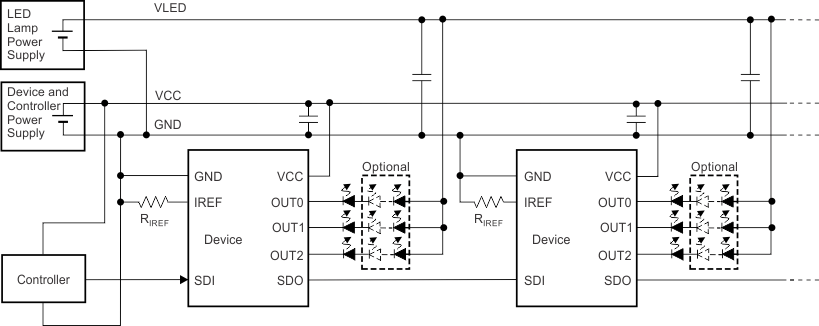 Figure 24. No Internal Shunt Regulator Mode 2 Typical Application Circuit
9.2.2.1 Design Requirements
Table 5. Design Parameters
| DESIGN PARAMETER | EXAMPLE VALUE |
|---|---|
| Input voltage range for VCC | 3.0 V to 5.5 V |
| Input voltage range for LED lamp | LED forward voltage (VF) × the number of LED lamps + 1 V; maximum voltage is 24 V |
| SDI voltage range | Low level = GND, high level = VCC |
| SDI data frequency | 100 kbps to 3 Mbps |
9.2.2.2 Detailed Design Procedure
The OUTn (n = 0 to 2) constant output current is set by an external resistor connected between the device IREF and GND pins. Use Equation 1 to calculate the requirements for RIREF.
9.2.2.3 Application Curve
Six LEDs are connected in series to each output.

| VCC = 3.3 V | VLED = 21 V | RIREF = 2.7 kΩ | ||||
| SDI high = 3.3 V | GS data = 7FFh (50% on duty) | |||||
9.2.3 Internal Shunt Regulator Mode
This application uses the shunt regulator. The device VCC and LED lamp anode voltage are supplied from the same power supply. At least two LED lamps are connected in series.
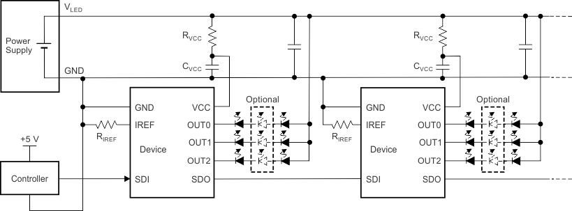
9.2.3.1 Design Requirements
Table 6. Design Parameters
| DESIGN PARAMETER | EXAMPLE VALUE |
|---|---|
| Input voltage range for VLED | 6 V to 24 V |
| SDI voltage range | Low level = GND, high level = 5.0 V to 6.0 V |
| SDI data transfer rate | 100 kbps to 3 Mbps |
9.2.3.2 Detailed Design Procedure
The TLC5973 internally integrates a shunt regulator to regulate VCC voltage. Refer to Figure 27 for an application circuit that uses the internal shunt regulator through a resistor, RVCC. The recommended RVCC value can be calculated by Equation 2.

 Figure 27. Internal Shunt Regulator Mode Application Circuit
Table 7 shows the typical resistor value for several VLED voltages. Note that the CVCC value should be 0.1 μF.
Table 7. Resistor Example for Shunt Resistor versus LED Voltage(1)
| VLED (V) | RVCC (Ω) | RESISTOR WATTAGE (W) |
|---|---|---|
| 9 | 270 | 0.04 |
| 12 | 510 | 0.07 |
| 18 | 1000 | 0.15 |
| 24 | 1500 | 0.22 |
9.2.3.3 Application Curves
Six LEDs are connected in series to each output.

| VLED = 21 V | RIREF = 2.7 kΩ | RVCC = 1.2 kΩ |
| SDI high = 6 V | GS data = 7FFh (50% on duty) | |

| VLED = 21 V | RIREF = 2.7 kΩ | RVCC = 1.2 kΩ |
| SDI high = 6 V | GS data = 7FFh (50% on duty) | |