ZHCSIJ9A May 2009 – July 2018 TLC5952
PRODUCTION DATA.
- 1 特性
- 2 应用
- 3 说明
- 4 修订历史记录
- 5 Pin Configuration and Functions
- 6 Specifications
- 7 Parameter Measurement Information
- 8 Detailed Description
- 9 Power Supply Recommendations
- 10器件和文档支持
- 11机械、封装和可订购信息
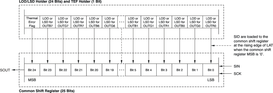
8.4.2.3 Status Information Data (SID)
The 25-bit word status information data (SID) contains the status of the LED open detection (LOD) or LED short detection (LSD), and thermal error flag (TEF). When the MSB of the common shift register is set to 0, the SID overwrites the common shift register data at the rising edge of LAT after the data in the common shift register are copied to the output on-off data latch. If the common shift register MSB is 1, the SID data are not copied to the common shift register.
After being copied into the common shift register, new SID data are not available until new data are written into the common shift register. If new data are not written, the LAT signal is ignored. To recheck SID data without changing the constant-current output on-off data, reprogram the common shift register with the same data that are currently programmed into the output on-off data latch. When LAT goes high, the output on-off data do not change, but new SID data are loaded into the common shift register. LOD, LSD, and TEF are shifted out of SOUT with each rising edge of SCLK.
 Figure 39. SID Load Assignment