ZHCSIJ9A May   2009  – July 2018 TLC5952

PRODUCTION DATA.  

  1. 特性
  2. 应用
  3. 说明
    1.     Device Images
      1.      典型应用电路(多个菊链式 TLC5952)
  4. 修订历史记录
  5. Pin Configuration and Functions
    1.     Pin Functions
  6. Specifications
    1. 6.1 Absolute Maximum Ratings
    2. 6.2 ESD Ratings
    3. 6.3 Recommended Operating Conditions
    4. 6.4 Thermal Information
    5. 6.5 Electrical Characteristics
    6. 6.6 Switching Characteristics
    7. 6.7 Typical Characteristics
  7. Parameter Measurement Information
    1. 7.1 Pin Equivalent Input and Output Schematic Diagrams
    2. 7.2 Test Circuits
  8. Detailed Description
    1. 8.1 Overview
    2. 8.2 Functional Block Diagram
    3. 8.3 Feature Description
      1. 8.3.1 Maximum Constant-Sink-Current Value
      2. 8.3.2 Global Brightness Control (BC) Function: Sink-Current Control
      3. 8.3.3 Constant-Current Output On-Off Control
    4. 8.4 Device Functional Modes
      1. 8.4.1 LOD, LSD, and TEF Operation
      2. 8.4.2 Register and Data Latch Configuration
        1. 8.4.2.1 Output On-Off Data Latch
        2. 8.4.2.2 Control-Data Latch
        3. 8.4.2.3 Status Information Data (SID)
        4. 8.4.2.4 LED-Open Detection (LOD), LED-Short Detection (LSD), And Thermal Error Flag (TEF)
        5. 8.4.2.5 Thermal Shutdown (TSD)
        6. 8.4.2.6 Noise Reduction
  9. Power Supply Recommendations
  10. 10器件和文档支持
    1. 10.1 接收文档更新通知
    2. 10.2 社区资源
    3. 10.3 商标
    4. 10.4 静电放电警告
    5. 10.5 术语表
  11. 11机械、封装和可订购信息

封装选项

机械数据 (封装 | 引脚)
散热焊盘机械数据 (封装 | 引脚)
订购信息

Register and Data Latch Configuration

The TLC5952 device has two writable data latches: the output on-off data latch and the control data latch. Both data latches are 24 bits in length. If the common shift register MSB is 0, the least significant 24 bits of data from the 25-bit common shift register are latched into the output on-off data latch. If the MSB is 1, the data are latched into the control data latch. Figure 37 shows the common shift register and the control data latch configuration.
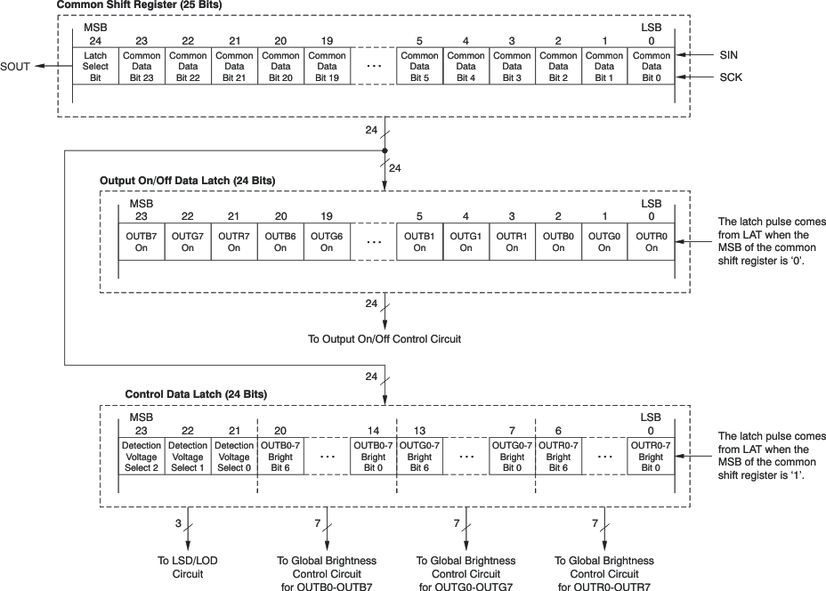
TLC5952 ai_config_common_reg_ctrl_latch_bvs129.gifFigure 37. Grayscale Shift Register and Data-Latch Configuration