ZHCSIJ9A May 2009 – July 2018 TLC5952
PRODUCTION DATA.
- 1 特性
- 2 应用
- 3 说明
- 4 修订历史记录
- 5 Pin Configuration and Functions
- 6 Specifications
- 7 Parameter Measurement Information
- 8 Detailed Description
- 9 Power Supply Recommendations
- 10器件和文档支持
- 11机械、封装和可订购信息
6.6 Switching Characteristics
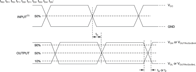
At TA = –40°C to 85°C, VCC = 3 V to 5.5 V, CL = 15 pF, RL = 120 Ω, RIREF = 1.5 kΩ, and VLED = 5 V, unless otherwise noted. Typical values are at TA = 25°C and VCC = 3.3 V.| PARAMETER | TEST CONDITIONS | MIN | TYP | MAX | UNIT | |
|---|---|---|---|---|---|---|
| tR0 | Rise time | SOUT | 6 | 15 | ns | |
| tR1 | OUTR0–OUTR7, OUTG0–OUTG7, OUTB0–OUTB7, BCR, -G, -B = 7Fh | 10 | 30 | ns | ||
| tF0 | Fall time | SOUT | 6 | 15 | ns | |
| tF1 | OUTR0–OUTR7, OUTG0–OUTG7, OUTB0–OUTB7, BCR, -G, -B = 7Fh | 10 | 30 | ns | ||
| tD0 | Propagation delay time(1) | SCLK↑ to SOUT | 8 | 20 | ns | |
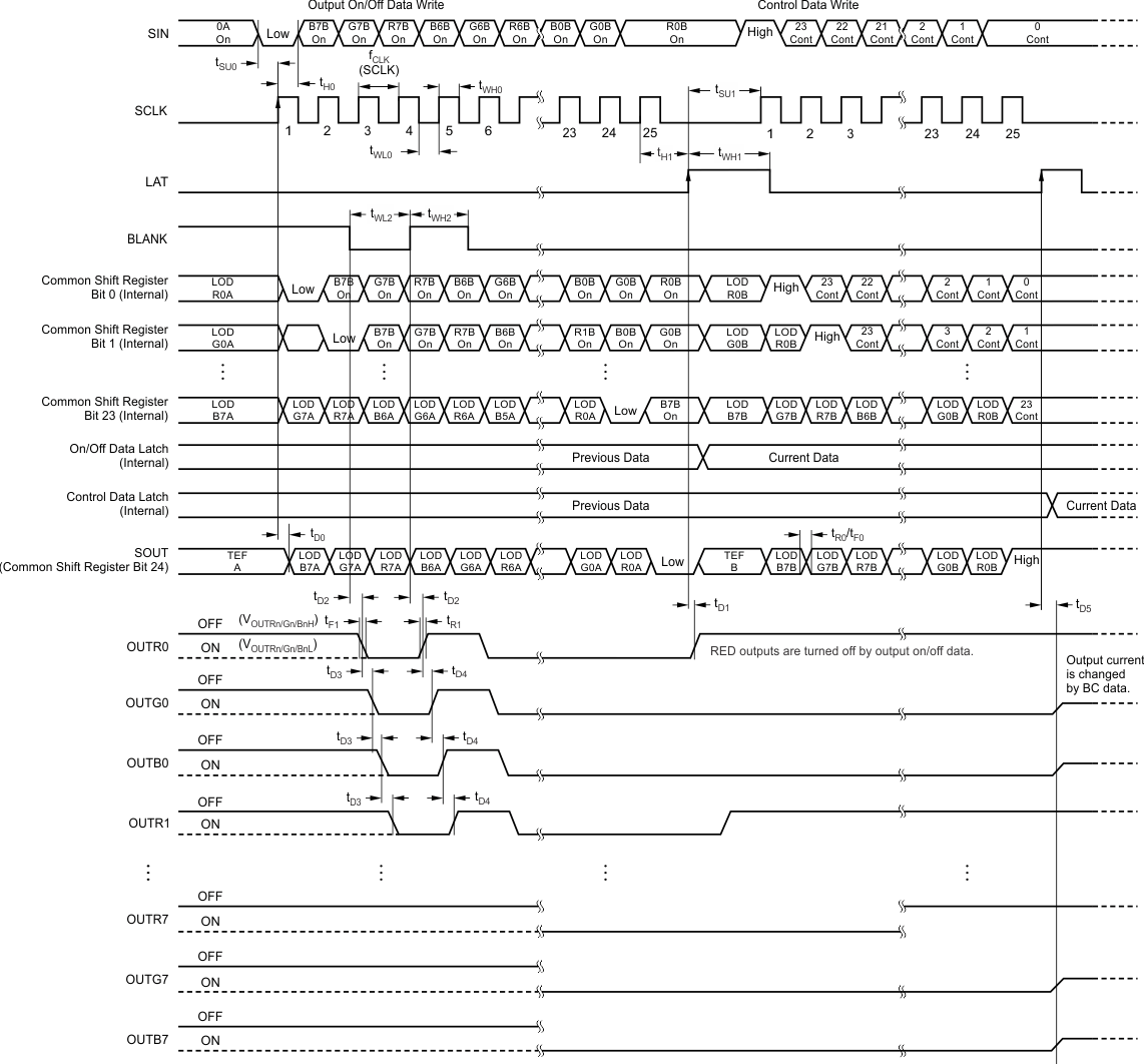
| tD1 | LAT↑ to OUTR0 on-off, BCR, -G, -B = 7Fh | 22 | 45 | ns | ||
| tD2 | BLANK↓↑ to OUTR0 on-off, BCR, -G, -B = 7Fh | 15 | 30 | ns | ||
| tD3 | OUTRn on to OUTGn on, OUTGn on to OUTBn on,
OUTBn on to OUTRn + 1 on, BCR, -G, -B = 7Fh |
3 | 6 | ns | ||
| tD4 | OUTRn off to OUTGn off, OUTGn off to OUTBn off,
OUTBn off to OUTRn + 1 off, BCR, -G, -B = 7Fh |
3 | 6 | ns | ||
| tD5 | LAT↑ to IOUTn changing by global brightness control (BC data are 0Ch–72h or 72h–0Ch) | 20 | 50 | ns | ||
| tON_ERR | Output on-time error(2) | On-off latched data = 1, BCR, -G, -B = 7Fh, 20 ns BLANK low level one-shot pulse input | –11 | 5 | ns | |
(1) Propagation delay, tD3 (OUTRn on to OUTGn on, OUTGn on to OUTBn on, OUTBn on to OUTRn + 1 on) is calculated by the formula:
tD3 (ns) = (the propagation delay between OUTR0 to OUTB7 = on) / 23
tD4 (OUTRn to OUTGn = off, OUTGn to OUTBn = off, OUTBn to OUTRn + 1 = off) is calculated by the formula:
tD4 (ns) = (the propagation delay between OUTR0 to OUTB7 = off) / 23
tD3 (ns) = (the propagation delay between OUTR0 to OUTB7 = on) / 23
tD4 (OUTRn to OUTGn = off, OUTGn to OUTBn = off, OUTBn to OUTRn + 1 = off) is calculated by the formula:
tD4 (ns) = (the propagation delay between OUTR0 to OUTB7 = off) / 23
(2) Output on-time error is calculated by the formula: tON_ERR (ns) = tOUT_ON – BLANK low-level pulse duration. tOUT_ON is the actual on-time of the constant current output.

NOINDENT:
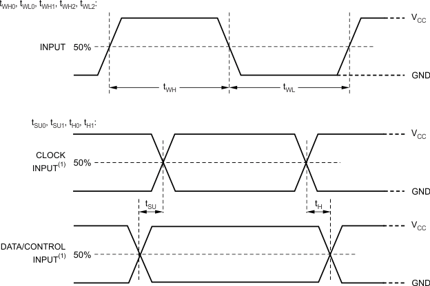
Input pulse rise and fall time is 1 ns to 3 ns.
