SLVS581B September 2006 – June 2015 TL5209
PRODUCTION DATA.
- 1 Features
- 2 Applications
- 3 Description
- 4 Typical Application Schematic
- 5 Revision History
- 6 Pin Configuration and Functions
- 7 Specifications
- 8 Detailed Description
- 9 Application and Implementation
- 10Power Supply Recommendations
- 11Layout
- 12Device and Documentation Support
- 13Mechanical, Packaging, and Orderable Information
7 Specifications
7.1 Absolute Maximum Ratings(1)
over operating free-air temperature range (unless otherwise noted)| MIN | MAX | UNIT | |||
|---|---|---|---|---|---|
| VI | Continuous input voltage | –20 | 20 | V | |
| VO | Output voltage | 7.5 | V | ||
| Tstg | Storage temperature | –65 | 150 | °C | |
(1) Stresses beyond those listed under Absolute Maximum Ratings may cause permanent damage to the device. These are stress ratings only, and functional operation of the device at these or any other conditions beyond those indicated under Recommended Operating Conditions is not implied. Exposure to absolute-maximum-rated conditions for extended periods may affect device reliability.
7.2 ESD Ratings
| VALUE | UNIT | |||
|---|---|---|---|---|
| V(ESD) | Electrostatic discharge | Human body model (HBM), per ANSI/ESDA/JEDEC JS-001(1) | ±2500 | V |
| Charged device model (CDM), per JEDEC specification JESD22-C101(2) | ±1000 | |||
(1) JEDEC document JEP155 states that 500-V HBM allows safe manufacturing with a standard ESD control process.
(2) JEDEC document JEP157 states that 250-V CDM allows safe manufacturing with a standard ESD control process.
7.3 Recommended Operating Conditions
| MIN | MAX | UNIT | ||
|---|---|---|---|---|
| VI | Input voltage | 2.5 | 16 | V |
| VO | Output voltage | 6.5 | V | |
| VEN | Enable input voltage | 0 | VI | V |
| TJ | Operating junction temperature | –40 | 125 | °C |
7.4 Thermal Information
| THERMAL METRIC(1) | TL5209 | UNIT | |
|---|---|---|---|
| D [SOIC] | |||
| 8 PINS | |||
| RθJA | Junction-to-ambient thermal resistance | 116.1 | °C/W |
| RθJC(top) | Junction-to-case (top) thermal resistance | 61.6 | °C/W |
| RθJB | Junction-to-board thermal resistance | 56.3 | °C/W |
| ψJT | Junction-to-top characterization parameter | 14.9 | °C/W |
| ψJB | Junction-to-board characterization parameter | 55.8 | °C/W |
| RθJC(bot) | Junction-to-case (bottom) thermal resistance | n/a | °C/W |
(1) For more information about traditional and new thermal metrics, see the Semiconductor and IC Package Thermal Metrics application report, SPRA953.
7.5 Electrical Characteristics
VIN = VOUT + 1 V, COUT = 4.7 μF, IOUT = 1 mA, full range TJ = –40°C to 125°C| PARAMETER | TEST CONDITIONS | TJ | MIN | TYP | MAX | UNIT | |
|---|---|---|---|---|---|---|---|
| Output voltage accuracy | VOUT = 2.5 V for ADJ only | 25°C | –1% | 1% | |||
| –40°C to 125°C | –2% | 2% | |||||
| αVOUT | Output voltage temperature coefficient | –40°C to 125°C | 40 | ppm/°C | |||
| Line regulation | VIN = (VOUT + 1 V) to 16 V | 25°C | 0.009 | 0.05 | %/V | ||
| –40°C to 125°C | 0.1 | ||||||
| Load regulation | IOUT = 1 mA to 500 mA(1) | 25°C | 0.05% | 0.5% | |||
| –40°C to 125°C | 0.7% | ||||||
| VIN – VOUT | Dropout voltage(2) | IOUT = 1 mA | 25°C | 45 | 60 | mV | |
| –40°C to 125°C | 80 | ||||||
| IOUT = 50 mA | 25°C | 115 | 175 | ||||
| –40°C to 125°C | 250 | ||||||
| IOUT = 100 mA | 25°C | 150 | 250 | ||||
| –40°C to 125°C | 300 | ||||||
| IOUT = 500 mA | 25°C | 350 | 500 | ||||
| –40°C to 125°C | 600 | ||||||
| IQ | Quiescent current | VEN ≥ 3 V, IOUT = 1 mA | 25°C | 100 | 140 | μA | |
| –40°C to 125°C | 170 | ||||||
| VEN ≥ 3 V, IOUT = 50 mA | 25°C | 350 | 650 | ||||
| –40°C to 125°C | 900 | ||||||
| VEN ≥ 3 V, IOUT = 100 mA | 25°C | 1.2 | 2 | mA | |||
| –40°C to 125°C | 3 | ||||||
| VEN ≥ 3 V, IOUT = 500 mA | 25°C | 8 | 20 | ||||
| –40°C to 125°C | 25 | ||||||
| Imin | Minimum load current(5) | –40°C to 125°C | 1 | mA | |||
| ISD | Shutdown current | VEN ≤ 0.4 V | 25°C | 0.05 | 3 | μA | |
| VEN ≤ 0.18 V | 25°C | 0.1 | |||||
| –40°C to 125°C | 8 | ||||||
| Ripple rejection | f = 120 Hz | 25°C | 75 | dB | |||
| ILIMIT | Current limit | VOUT = 0 V | 25°C | 700 | 900 | mA | |
| –40°C to 125°C | 1000 | ||||||
| ΔVOUT/ΔPD | Thermal regulation(3) | VIN = 16 V, 500-mA load pulse for t = 10 ms | 25°C | 0.05 | %/W | ||
| Vn | Output noise | VOUT = 2.5 V, IOUT = 50 mA, COUT = 2.2 μF, CBYP = 0 | 25°C | 500 | nV/√Hz | ||
| IOUT = 50 mA, COUT = 2.2 μF, CBYP = 470 pF(4) | 25°C | 300 | |||||
| VEN | Enable logic voltage | VEN = logic LOW (shutdown) | 25°C | 0.4 | V | ||
| –40°C to 125°C | 0.18 | ||||||
| VEN = logic HIGH (enabled) | 25°C | 2 | |||||
| IEN | Enable input current | VEN ≤ 0.4 V (shutdown) | 25°C | 0.01 | –1 | μA | |
| VEN ≤ 0.18 V (shutdown) | –40°C to 125°C | 0.01 | –2 | ||||
| VEN ≥ 2 V (enabled) | 25°C | 5 | 20 | ||||
| –40°C to 125°C | 25 | ||||||
(1) Low duty cycle testing is used to maintain the junction temperature as close to the ambient temperature as possible. Changes in output voltage due to thermal effects are covered separately by the thermal regulation specification.
(2) Dropout is defined as the input to output differential at which the output drops 2% below its nominal value measured at 1-V differential.
(3) Thermal regulation is defined as the change in output voltage at a specified time after a change in power dissipation is applied, excluding line and load regulation effects.
(4) CBYP is optional and connected to the BYP/ADJ pin.
(5) For stability across the input voltage and temperature. For ADJ versions, the minimum current can be set by R1 and R2.
7.6 Typical Characteristics
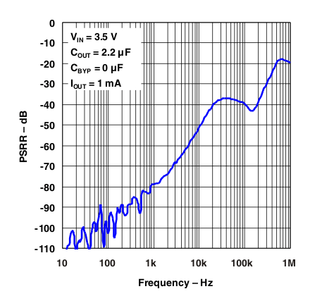 Figure 1. Power Supply Rejection Ratio
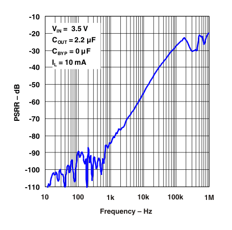 Figure 3. Power Supply Rejection Ratio
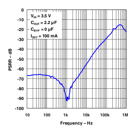 Figure 5. Power Supply Rejection Ratio
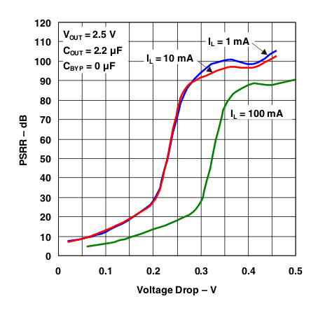 Figure 7. Power Supply Ripple Rejection vs Voltage Drop
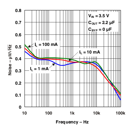 Figure 9. Noise Performance
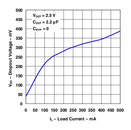 Figure 11. Dropout Voltage vs Load Current
 Figure 13. Ground Current vs Load Current
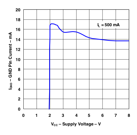 Figure 15. Ground Current vs Supply Voltage
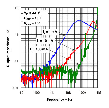 Figure 17. Output Impedance vs Frequency
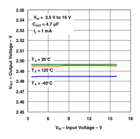 Figure 19. Output Voltage vs Input Voltage
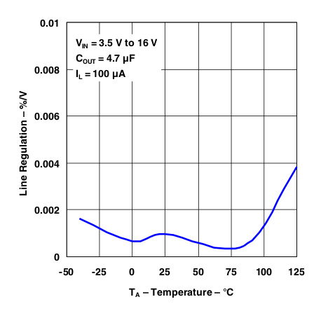 Figure 21. Line Regulation
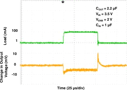 Figure 23. Load Transient Response
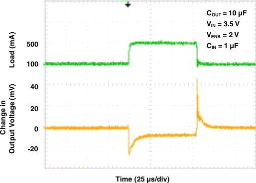 Figure 25. Load Transient Response
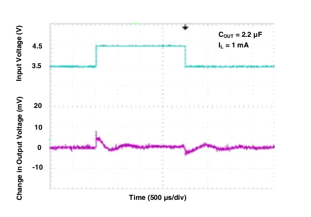 Figure 27. Line Transient Response
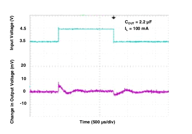 Figure 29. Line Transient Response
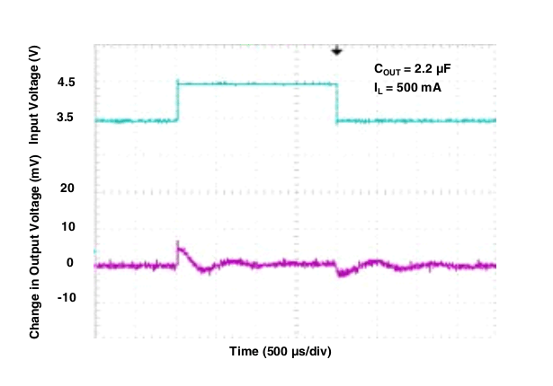 Figure 31. Line Transient Response
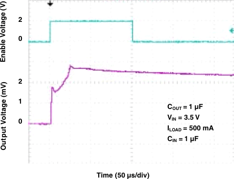 Figure 33. Turnon Time
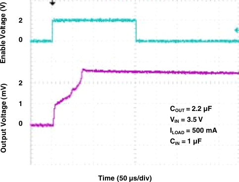 Figure 35. Turnon Time
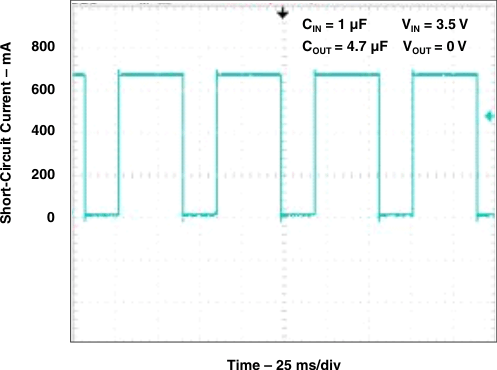 Figure 37. Short-Circuit Current vs Time
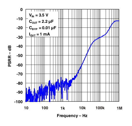 Figure 2. Power Supply Rejection Ratio
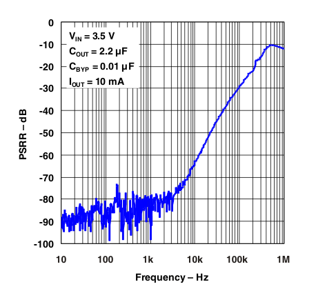 Figure 4. Power Supply Rejection Ratio
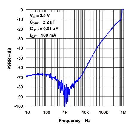 Figure 6. Power Supply Rejection Ratio
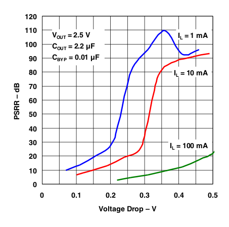 Figure 8. Power Supply Ripple Rejection vs Voltage Drop
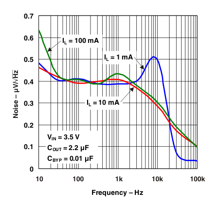 Figure 10. Noise Performance
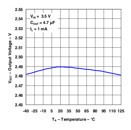 Figure 12. Output Voltage vs Temperature
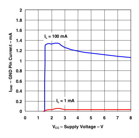 Figure 14. Ground Current vs Supply Voltage
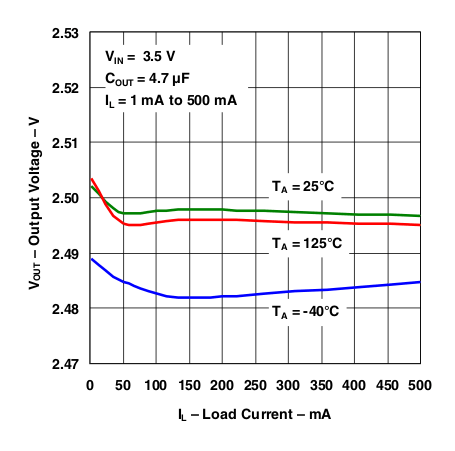 Figure 16. Output Voltage vs Load Current
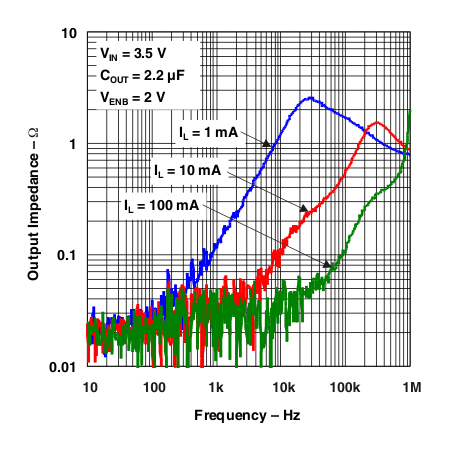 Figure 18. Output Impedance vs Frequency
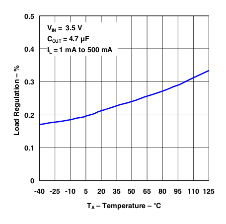 Figure 20. Load Regulation
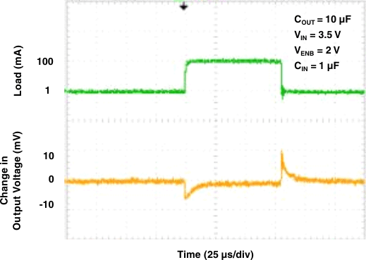 Figure 22. Load Transient Response
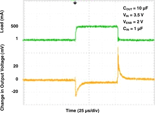 Figure 24. Load Transient Response
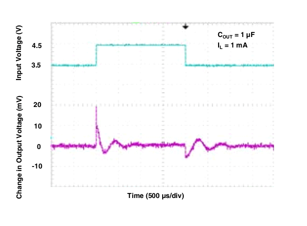 Figure 26. Line Transient Response
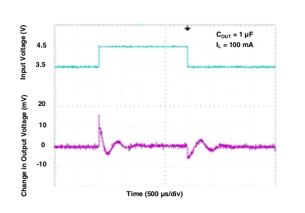 Figure 28. Line Transient Response
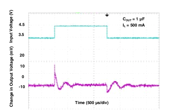 Figure 30. Line Transient Response
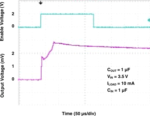 Figure 32. Turnon Time
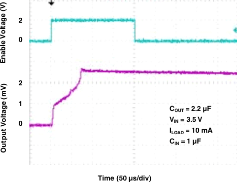 Figure 34. Turnon Time
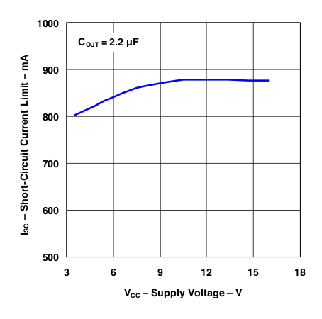 Figure 36. Short-Circuit Current vs Supply Voltage
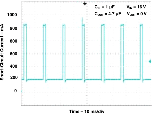 Figure 38. Short-Circuit Current vs Time