SLVS581B September 2006 – June 2015 TL5209
PRODUCTION DATA.
- 1 Features
- 2 Applications
- 3 Description
- 4 Typical Application Schematic
- 5 Revision History
- 6 Pin Configuration and Functions
- 7 Specifications
- 8 Detailed Description
- 9 Application and Implementation
- 10Power Supply Recommendations
- 11Layout
- 12Device and Documentation Support
- 13Mechanical, Packaging, and Orderable Information
8 Detailed Description
8.1 Overview
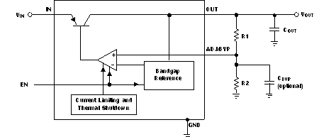
The TL5209 device is a low-dropout (LDO) regulator with an input voltage range from 2.5 V to 16 V and a maximum output current of 500 mA. The output voltage can be adjusted using external resistors (R1 and R2) and has an accuracy of 1% to 2% depending on the ambient temperature. The maximum voltage drop across the device varies from 10 mV to 500 mV depending on the current load at the output.
8.2 Functional Block Diagram
 Figure 39. Low-Noise Adjustable Regulator
8.3 Feature Description
8.3.1 Enable and Shutdown
The EN pin is CMOS-logic compatible. When EN is held high (>2 V), the regulator is active. Likewise, applying a low signal (<0.4 V at 25°C) to EN or leaving it open shuts down the regulator. If the enable or shutdown feature is not needed, EN should be tied to VIN.
8.4 Device Functional Modes
The table below lists the expected value of VOUT as determined by the EN pin.
Table 1. VOUT Function Table
| EN (Control Input) | VOUT |
|---|---|
| L | Open |
| H | 1.242 V × (1 + R2/R1) |