SLVS581B September 2006 – June 2015 TL5209
PRODUCTION DATA.
- 1 Features
- 2 Applications
- 3 Description
- 4 Typical Application Schematic
- 5 Revision History
- 6 Pin Configuration and Functions
- 7 Specifications
- 8 Detailed Description
- 9 Application and Implementation
- 10Power Supply Recommendations
- 11Layout
- 12Device and Documentation Support
- 13Mechanical, Packaging, and Orderable Information
9 Application and Implementation
NOTE
Information in the following applications sections is not part of the TI component specification, and TI does not warrant its accuracy or completeness. TI’s customers are responsible for determining suitability of components for their purposes. Customers should validate and test their design implementation to confirm system functionality.
9.1 Application Information
9.1.1 Low-Voltage Operation
When using the TL5209 in voltage-sensitive applications, special considerations are required. If appropriate output and bypass capacitors are not chosen properly, these devices may experience a temporary overshoot of their nominal voltages.
At start-up, the full input voltage is initially applied across the regulator pass transistor, causing it to be temporarily fully turned on. By contrast, the error amplifier and voltage-reference circuits, being powered from the output, are not powered up as fast. To slow down the output ramp and give the error amplifier time to respond, select larger values of output and bypass capacitors. The longer ramp time of the output allows the regulator enough time to respond and keeps the output from overshooting its nominal value.
To prevent an overshoot when starting up into a light load (≉100 μA), TI recommends 4.7-μF and 470-pF capacitors for the output and bypass capacitors, respectively. At higher loads, 10-μF and 470-pF capacitors should be used.
If the application is not very sensitive to regulator overshoot, both the output capacitor and bypass capacitor (if applicable) can be reduced.
9.2 Typical Application

9.2.1 Design Requirements
For this design example, use the parameters listed in Table 2 as the input parameters.
Table 2. Design Parameters
| DESIGN PARAMETER | EXAMPLE VALUE |
|---|---|
| VIN | 5 V |
| R1 | 100 kΩ |
| Load current | 500 mA |
| Desired VOUT | 3.3 V |
9.2.2 Detailed Design Procedure
9.2.2.1 Setting the Output Voltage
The TL5209 develops a 1.242-V reference voltage, VREF, between the output and the adjust terminal. As shown in Figure 40, this voltage is applied across resistor R1 to generate a constant current. The current IADJ from the ADJ terminal could introduce DC offset to the output. Because, this offset is very small (about 50 nA), it can be ignored. The constant current then flows through the output set resistor R2 and sets the output voltage to the desired level. Equation 1 is used for calculating VOUT:
With an R1 resistance of 100 kΩ and a desired output voltage of 3.3 V, the value for R2 can be calculated:
Therefore, with an R2 resistance of 165.7 kΩ, the output voltage can be set to 3.3 V.
The TL5209 adjustable output should not be adjusted above 6.75 V ± 10% due to the internal Zener diode clamping the output voltage above 6.75 V. Although IADJ is very small, R2 should be limited to less than 470 kΩ for optimum performance.
9.2.2.2 Input Capacitor
If the input of the regulator is located more than ten inches from the power-supply filter, or if a battery is used to power the regulator, TI recommends a minimum 1-μF input capacitor.
9.2.2.3 Output Capacitor
As with all PNP regulators, an output capacitor is needed for stability. The required minimum size of this output capacitor depends on several factors, one of which is whether a bypass capacitor is used.
- With no bypass capacitor, TI recommends a minimum COUT of 1 μF.
- With a bypass capacitor of 470 pF (see Figure 40), TI recommends a minimum COUT of 2.2 μF.
- Larger values of COUT are beneficial, because they improve the regulator transient response.
Another factor that can determine the minimum size of the output capacitor is the load current. At low loads, a smaller output capacitor is needed for stability.
The equivalent series resistance (ESR) of the output capacitor also can affect regulator stability. COUT should have an ESR of ≉1 Ω, and it should have a resonant frequency greater than 1 MHz. Too low of an ESR can cause the output to have a low-amplitude oscillation and/or underdamped transient response. Most tantalum or aluminum electrolytic capacitors can be used for the output capacitors. However, care must be taken at low temperatures, because aluminum electrolytics use electrolytes that can freeze at low temperature (≉ –30°C). Solid tantalum capacitors do not exhibit this problem and should be used below –25°C.
9.2.2.4 Bypass Capacitor
An optional bypass capacitor, CBYP, can be externally connected to the regulator through the BYP pin for improved noise performance. Connected to the internal voltage divider and the error amplifier of the regulator, this bypass capacitor filters the noise of the internal reference and reduces the noise effects on the error amplifier. The overall result is a significant drop in output noise of the regulator. TI recommends a 470-pF bypass capacitor.
Adding a bypass capacitor has several effects on the regulator that must be taken into account. First, the bypass capacitor reduces the phase margin of the regulator and, thus, the minimum COUT needs to be increased to 2.2 μF, as previously mentioned. Second, upon start-up of the regulator, the bypass capacitor has an effect on the regulator turnon time. If a slow ramp-up of the output is needed, larger values of CBYP should be used. Conversely, if a fast ramp-up of the output is needed, use a smaller CBYP or none at all.
If a bypass capacitor is not needed, BYP should be left open.
9.2.3 Application Curves
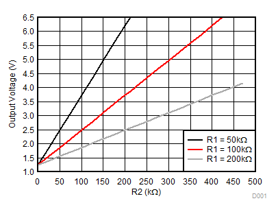
Figure 41 shows the expected output voltage versus R2 for various values of R1.
 Figure 41. Expected Output Voltage vs R2 Resistance