SLOS823D December   2012  – March 2020 THS4531A

PRODUCTION DATA.  

  1. Features
  2. Applications
  3. Description
    1.     1-kHz FFT Plot on Audio Analyzer
  4. Revision History
  5. Related Products
  6. Pin Configuration and Functions
    1.     Pin Functions
  7. Specifications
    1. 7.1 Absolute Maximum Ratings
    2. 7.2 ESD Ratings
    3. 7.3 Recommended Operating Conditions
    4. 7.4 Thermal Information
    5. 7.5 Electrical Characteristics: VS = 2.7 V
    6. 7.6 Electrical Characteristics: VS = 5 V
    7. 7.7 Typical Characteristics
      1. 7.7.1 Typical Characteristics: VS = 2.7 V
      2. 7.7.2 Typical Characteristics: VS = 5 V
  8. Detailed Description
    1. 8.1 Overview
    2. 8.2 Functional Block Diagram
    3. 8.3 Feature Description
      1. 8.3.1 Input Common-Mode Voltage Range
        1. 8.3.1.1 Setting the Output Common-Mode Voltage
      2. 8.3.2 Power Down
    4. 8.4 Device Functional Modes
  9. Application and Implementation
    1. 9.1 Application Information
      1. 9.1.1  Frequency Response, and Output Impedance
      2. 9.1.2  Distortion
      3. 9.1.3  Slew Rate, Transient Response, Settling Time, Overdrive, Output Voltage, and Turnon and Turnoff Time
      4. 9.1.4  Common-Mode and Power Supply Rejection
      5. 9.1.5  VOCM Input
      6. 9.1.6  Balance Error
      7. 9.1.7  Single-Supply Operation
      8. 9.1.8  Low-Power Applications and the Effects of Resistor Values on Bandwidth
      9. 9.1.9  Driving Capacitive Loads
      10. 9.1.10 Audio Performance
      11. 9.1.11 Audio On and Off Pop Performance
    2. 9.2 Typical Applications
      1. 9.2.1 SAR ADC Performance: THS4531A and ADS8321 Combined Performance
        1. 9.2.1.1 Design Requirements
        2. 9.2.1.2 Detailed Design Procedure
        3. 9.2.1.3 Application Curve
      2. 9.2.2 Audio ADC Driver Performance: THS4531A and PCM4204 Combined Performance
        1. 9.2.2.1 Detailed Design Procedure
        2. 9.2.2.2 Application Curves
      3. 9.2.3 SAR ADC Performance: THS4531A and ADS7945 Combined Performance
        1. 9.2.3.1 Design Requirements
        2. 9.2.3.2 Detailed Design Procedure
        3. 9.2.3.3 Application Curve
      4. 9.2.4 Differential-Input to Differential-Output Amplifier
        1. 9.2.4.1 AC-Coupled, Differential-Input to Differential-Output Design Issues
      5. 9.2.5 Single-Ended to Differential FDA Configuration
        1. 9.2.5.1 Input Impedance
      6. 9.2.6 Single-Ended Input to Differential Output Amplifier
        1. 9.2.6.1 AC-Coupled Signal Path Considerations for Single-Ended Input to Differential Output Conversion
        2. 9.2.6.2 DC-Coupled Input Signal Path Considerations for Single-Ended to Differential Conversion
        3. 9.2.6.3 Resistor Design Equations for the Single-Ended to Differential Configuration of the FDA
      7. 9.2.7 Differential Input to Single-Ended Output Amplifier
  10. 10Power Supply Recommendations
  11. 11Layout
    1. 11.1 Layout Guidelines
    2. 11.2 Layout Example
  12. 12Device and Documentation Support
    1. 12.1 Device Support
      1. 12.1.1 Third-Party Products Disclaimer
    2. 12.2 Documentation Support
    3. 12.3 Community Resources
    4. 12.4 Trademarks
    5. 12.5 Electrostatic Discharge Caution
    6. 12.6 Glossary
  13. 13Mechanical, Packaging, and Orderable Information

封装选项

机械数据 (封装 | 引脚)
散热焊盘机械数据 (封装 | 引脚)
订购信息

Typical Characteristics: VS = 2.7 V

Test conditions unless otherwise noted: VS+ = 2.7 V, VS– = 0 V, CM = open, VOUT = 2 Vpp, RF = 2 kΩ, RL = 2 kΩ Differential, G = 1 V/V, Single-Ended Input, Differential Output, Input and Output Referenced to mid-supply, TA ≈ 25°C, unless otherwise noted.
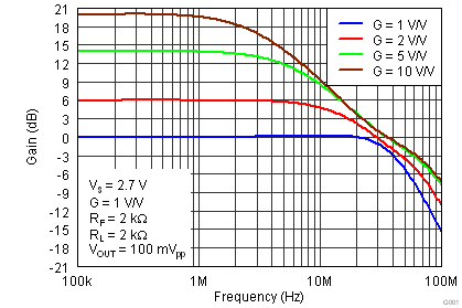
THS4531A G001_Small-Signal_Frequency_Response.png
Figure 1. Small-Signal Frequency Response
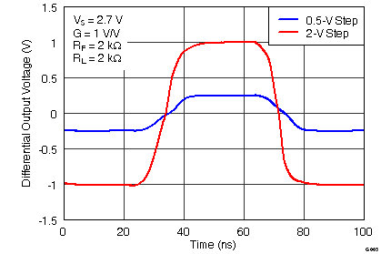
THS4531A G003_Large-_and_Small-Signal_Pulse_Response.png
Figure 3. Large- and Small-Signal Pulse Response
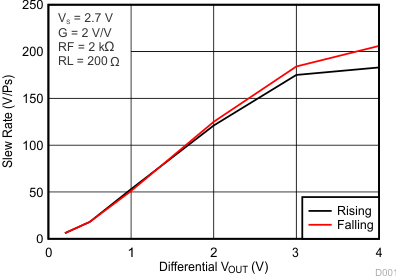
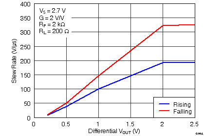
THS4531A NewFigure5.gif
Figure 5. Differential Slew Rate vs VOUT Step
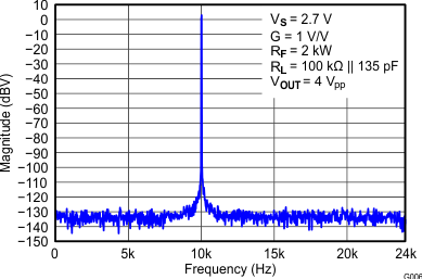
THS4531A g06.gif
Figure 7. 10-kHz FFT On Audio Analyzer
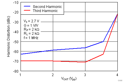
THS4531A G008_Harmonic_Distortion_vs_Output_Voltage_at_1MHz_RF=2k_RL=2k.png
Figure 9. Harmonic Distortion vs Output Voltage at 1 MHz
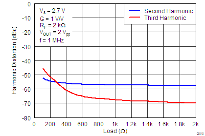
THS4531A G010_Harmonic_Distortion_vs_Load_at_1MHz_RF=2k.png
Figure 11. Harmonic Distortion vs Load at 1 MHz
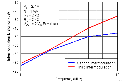
THS4531A G012_Two-Tone_Second-_and_Third-Order_Intermodulation_Distortion_vs_Frequency_RF=2k_RL=2k.png
Figure 13. Two-Tone, 2nd and 3rd Order Intermodulation
Distortion vs Frequency
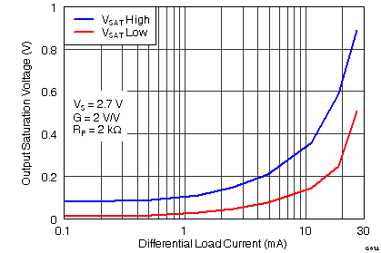
THS4531A G014_Single-Ended_Output_Saturation_Voltage_vs_Load_Current.png
Figure 15. Single-Ended Output Saturation Voltage vs Load Current
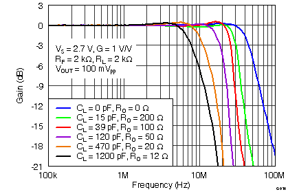
THS4531A G016_Frequency_Response_vs_CLOAD_RLOAD_=_2k.png
Figure 17. Frequency Response vs CLOAD
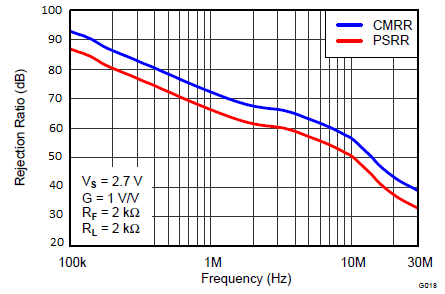
THS4531A fig19_slos823.png
Figure 19. Rejection Ratio vs Frequency
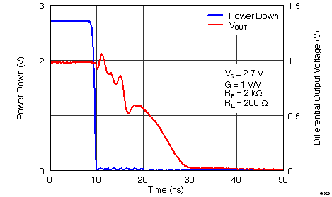
THS4531A G020_Turn_Off_Time_RF=2k_RL=200.png
Figure 21. Turnoff Time
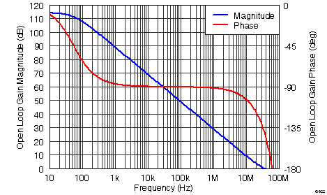
THS4531A G022_Main_Amplifier_Differential_Open-Loop_Gain_and_Phase.png
Figure 23. Main Amplifier Differential Open-Loop Gain and Phase vs Frequency
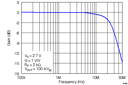
THS4531A G024_Vocm_Small-Signal_Frequency_Response_RF=2k.png
Figure 25. VOCM Small-Signal Frequency Response
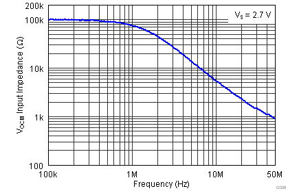
THS4531A G026_Vocm_Input_Impedance_vs_Frequency.png
Figure 27. VOCM Input Impedance vs Frequency
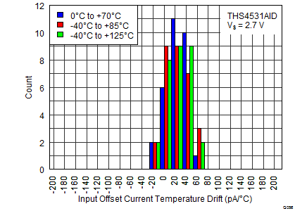
THS4531A Figure 30 IOS Drift 2_7V.png
Figure 29. Input Offset Current Temp Drift Histogram
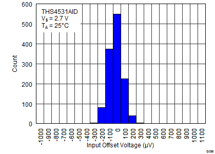
THS4531A Figure 32 VOS at 25C 2_7V.png
Figure 31. Input Offset Voltage Histogram
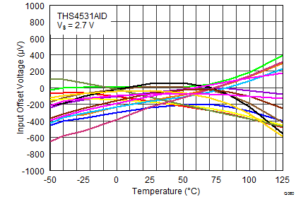
THS4531A Figure 34 VOS Over Temp 2_7V.png
Figure 33. Input Offset Voltage vs Temperature
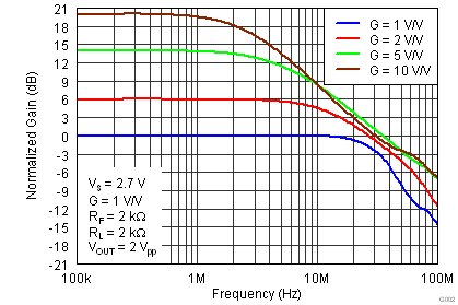
THS4531A G002_Large-Signal_Frequency_Response.png
Figure 2. Large-Signal Frequency Response
THS4531A G004_Slew_Rate_vs_Vout_Step_RL=200.png
Figure 4. Single-Ended Slew Rate vs VOUT Step
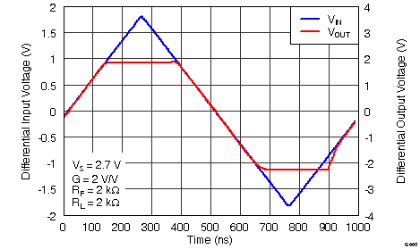
THS4531A G005_Overdrive_Recovery.png
Figure 6. Overdrive Recovery
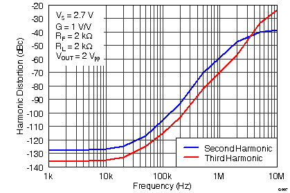
THS4531A G007_Harmonic_Distortion_vs_Frequency_RF=2k_RL=2k.png
Figure 8. Harmonic Distortion vs Frequency
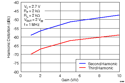
THS4531A G009_Harmonic_Distortion_vs_Gain_at_1MHz_RF=2k_RL=2k.png
Figure 10. Harmonic Distortion vs Gain at 1 MHz
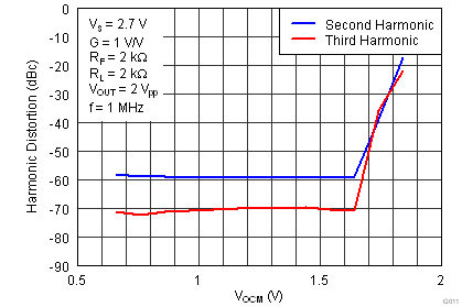
THS4531A G011_Harmonic_Distortion_vs_Vocm_at_1MHz_RF=2k_RL=2k.png
Figure 12. Harmonic Distortion vs VOCM at 1 MHz
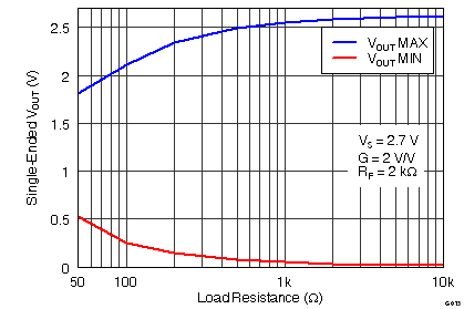
THS4531A G013_Single-Ended_Output_Voltage_Swing_vs_Load_Resistance.png
Figure 14. Single-Ended Output Voltage Swing vs Load Resistance
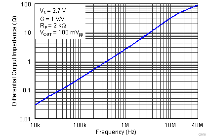
THS4531A G015_Main_Amplifier_Differential_Output_Impedance_vs_Frequency.png
Figure 16. Main Amplifier Differential Output Impedance vs Frequency
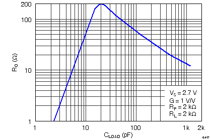
THS4531A G017_RO_vs_CLOAD_RLOAD_=_2k.png
Figure 18. RO vs CLOAD
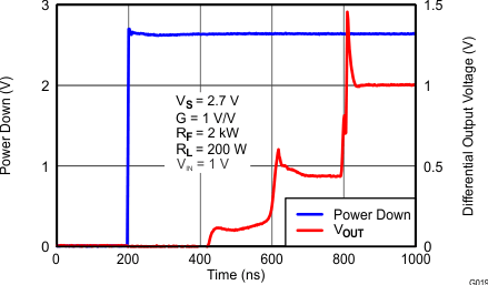
THS4531A g19.gif
Figure 20. Turnon Time
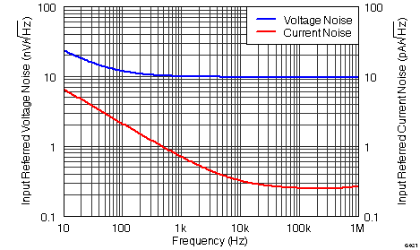
THS4531A G021_Input-Referred_Voltage_Noise_and_Current_Noise_Spectral_Density.png
Figure 22. Input-Referred Voltage Noise and Current Noise Spectral Density
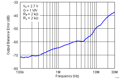
THS4531A G023_Output_Balance_Error_vs_Frequency_RF=2k_RL=1k.png
Figure 24. Output Balance Error vs Frequency
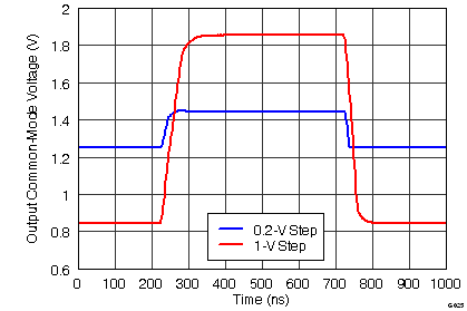
THS4531A G025_Vocm_Large-_and_Small_Signal_Pulse_Response_RF=2k.png
Figure 26. VOCM Large- and Small Signal Pulse Response
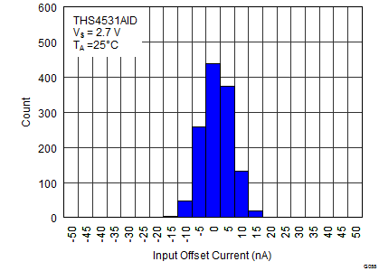
THS4531A Figure 29 IOS at 25C 2_7V.png
Figure 28. Input Offset Current Histogram
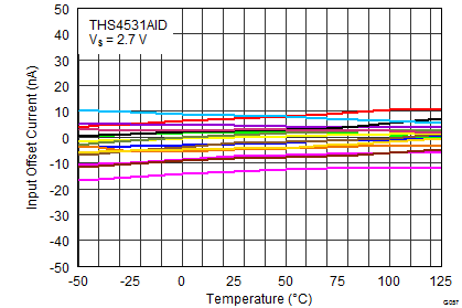
THS4531A Figure 31 IOS Over Temp 2_7V.png
Figure 30. Input Offset Current vs Temperature
THS4531A Figure 33 VOS Drift 2_7V.png
Figure 32. Input Offset Voltage Temp Drift Histogram