SLOS823D December 2012 – March 2020 THS4531A
PRODUCTION DATA.
- 1 Features
- 2 Applications
- 3 Description
- 4 Revision History
- 5 Related Products
- 6 Pin Configuration and Functions
- 7 Specifications
- 8 Detailed Description
-
9 Application and Implementation
- 9.1
Application Information
- 9.1.1 Frequency Response, and Output Impedance
- 9.1.2 Distortion
- 9.1.3 Slew Rate, Transient Response, Settling Time, Overdrive, Output Voltage, and Turnon and Turnoff Time
- 9.1.4 Common-Mode and Power Supply Rejection
- 9.1.5 VOCM Input
- 9.1.6 Balance Error
- 9.1.7 Single-Supply Operation
- 9.1.8 Low-Power Applications and the Effects of Resistor Values on Bandwidth
- 9.1.9 Driving Capacitive Loads
- 9.1.10 Audio Performance
- 9.1.11 Audio On and Off Pop Performance
- 9.2
Typical Applications
- 9.2.1 SAR ADC Performance: THS4531A and ADS8321 Combined Performance
- 9.2.2 Audio ADC Driver Performance: THS4531A and PCM4204 Combined Performance
- 9.2.3 SAR ADC Performance: THS4531A and ADS7945 Combined Performance
- 9.2.4 Differential-Input to Differential-Output Amplifier
- 9.2.5 Single-Ended to Differential FDA Configuration
- 9.2.6 Single-Ended Input to Differential Output Amplifier
- 9.2.7 Differential Input to Single-Ended Output Amplifier
- 9.1
Application Information
- 10Power Supply Recommendations
- 11Layout
- 12Device and Documentation Support
- 13Mechanical, Packaging, and Orderable Information
封装选项
机械数据 (封装 | 引脚)
散热焊盘机械数据 (封装 | 引脚)
- RUN|10
订购信息
9.1 Application Information
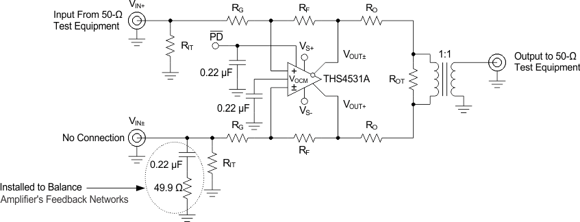
Figure 70 shows the general test circuit built on the EVM that was used for testing the THS4531A. For simplicity, power supply decoupling is not shown – see Layout for recommendations. Depending on the test conditions, component values are changed per Table 4 and Table 5, or as otherwise noted. Some of the signal generators used are AC-coupled 50-Ω sources and a 0.22-µF capacitor and 49.9-Ω resistor to ground are inserted across RIT on the un-driven or alternate input as shown to balance the circuit. A split-power supply is used to ease the interface to common lab test equipment, but if properly biased, the amplifier can be operated single-supply as described in the applications section with no impact on performance. For most of the tests, the devices are tested with single ended input and a transformer on the output to convert the differential output to single ended because common lab test equipment have single ended inputs and outputs. Performance is the same or better with differential input and differential output.
 Figure 70. General Test Circuit
 Table 4. Gain Component Values for Single-Ended Input(1)
| GAIN | RF | RG | RIT |
|---|---|---|---|
| 1 V/V | 2 kΩ | 2 kΩ | 51.1 Ω |
| 2 V/V | 2 kΩ | 1 kΩ | 52.3 Ω |
| 5 V/V | 2 kΩ | 392 Ω | 53.6 Ω |
| 10 V/V | 2 kΩ | 187 Ω | 57.6 Ω |
Table 5. Load Component Values For 1:1 Differential to Single-Ended Output Transformer(1)
| RL | RO | ROT | ATTEN (dB) |
|---|---|---|---|
| 100 Ω | 25 Ω | open | 6 |
| 200 Ω | 84.5 Ω | 71.5 Ω | 16.7 |
| 500 Ω | 237 Ω | 56.2 Ω | 25.6 |
| 1 kΩ | 487 Ω | 52.3 Ω | 31.8 |
| 2 kΩ | 976 Ω | 51.1 Ω | 38 |
Because of the voltage divider on the output formed by the load component values, the output of the amplifier is attenuated. The column ATTEN in Table 5 shows the attenuation expected from the resistor divider. When using a transformer at the output as shown in Figure 70, the signal has slightly more loss because of transformer insertion loss, and these numbers are approximate. The standard output load used for most tests is 2 kΩ with associated 38 dB of loss.