ZHCSCR9C September 2014 – February 2017 TCA9534A
PRODUCTION DATA.
- 1 特性
- 2 应用
- 3 说明
- 4 修订历史记录
- 5 Pin Configuration and Functions
- 6 Specifications
- 7 Parameter Measurement Information
- 8 Detailed Description
- 9 Application and Implementation
- 10Power Supply Recommendations
- 11Layout
- 12器件和文档支持
- 13机械、封装和可订购信息
封装选项
机械数据 (封装 | 引脚)
散热焊盘机械数据 (封装 | 引脚)
- DW|16
订购信息
8.6.3.1.2 Reads
Reading from a slave is very similar to writing, but requires some additional steps. In order to read from a slave, the master must first instruct the slave which register it wishes to read from. This is done by the master starting off the transmission in a similar fashion as the write, by sending the address with the R/W bit equal to 0 (signifying a write), followed by the register address it wishes to read from. When the slave acknowledges this register address, the master sends a START condition again, followed by the slave address with the R/W bit set to 1 (signifying a read). This time, the slave acknowledges the read request, and the master releases the SDA bus but continues supplying the clock to the slave. During this part of the transaction, the master becomes the master-receiver, and the slave becomes the slave-transmitter.
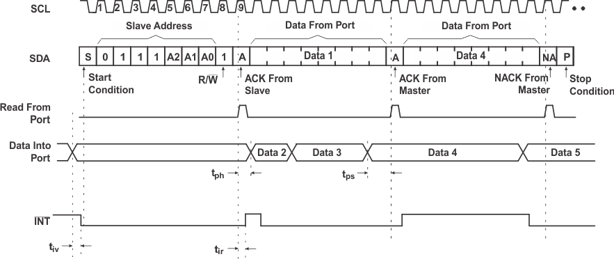
The master continues to send out the clock pulses, but releases the SDA line so that the slave can transmit data. At the end of every byte of data, the master sends an ACK to the slave, letting the slave know that it is ready for more data. When the master has received the number of bytes it is expecting, it sends a NACK, signaling to the slave to halt communications and release the bus. The master follows this up with a STOP condition.
See Table 3 for the list of the internal registers and a description of each one.
If a read is requested by the master after a POR without first setting the command byte via a write, the device will NACK until a command byte-register address is set as described above.
Figure 31 shows an example of reading a single byte from a slave register.
 Figure 31. Read From Register
Data is clocked into the register on the rising edge of the ACK clock pulse. There is no limitation on the number of data bytes received in one read transmission, but when the final byte is received, the bus master must not acknowledge the data. See Figure 32.
