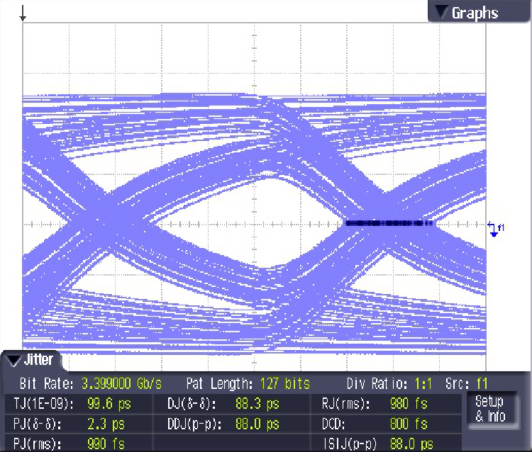
ZHCS794B February 2012 – August 2015 SN75DP126
PRODUCTION DATA.
- 1 特性
- 2 应用
- 3 说明
- 4 修订历史记录
- 5 说明 (续)
- 6 Pin Configuration and Functions
-
7 Specifications
- 7.1 Absolute Maximum Ratings
- 7.2 ESD Ratings
- 7.3 Recommended Operating Conditions
- 7.4 Thermal Information
- 7.5 Power Supply Electrical Characteristics
- 7.6 Main Link Input Electrical Characteristics
- 7.7 DisplayPort Main Link Output Electrical Characteristics
- 7.8 HDMI/DVI Main Link Output Electrical Characteristics
- 7.9 HPD/CAD/EN Electrical Characteristics
- 7.10 AUX/DDC/I2C Electrical Characteristics
- 7.11 DisplayPort Main Link Output Switching Characteristics
- 7.12 HDMI/DVI Main Link Switching Characteristics
- 7.13 HPD/CAD Switching Characteristics
- 7.14 AUX/DDC/I2C Switching Characteristics
- 7.15 Typical Characteristics
-
8 Detailed Description
- 8.1 Overview
- 8.2 Functional Block Diagram
- 8.3
Feature Description
- 8.3.1 Implementing the EN Signal
- 8.3.2 Hot Plug Detect (HPD) and Cable Adapter Detect (CAD) Description
- 8.3.3 OVS Function Description
- 8.3.4 AUX and DDC Configuration Details
- 8.3.5 Source-Side Main Link EQ Configuration Details
- 8.3.6 DP-HDMI Adaptor ID Buffer
- 8.3.7 GPU with a Unified AUX/DDC Configuration
- 8.3.8 GPU with Separate DDC and AUX Channels
- 8.4 Device Functional Modes
- 8.5 Register Maps
- 9 Application and Implementation
- 10Power Supply Recommendations
- 11Layout
- 12器件和文档支持
- 13机械、封装和可订购信息
7 Specifications
7.1 Absolute Maximum Ratings
over operating free-air temperature range (unless otherwise noted)(1)
(1) Stresses beyond those listed under Absolute Maximum Ratings may cause permanent damage to the device. These are stress ratings only, which do not imply functional operation of the device at these or any other conditions beyond those indicated under Recommended Operating Conditions. Exposure to absolute-maximum-rated conditions for extended periods may affect device reliability.
7.2 ESD Ratings
| VALUE | UNIT | |||
|---|---|---|---|---|
| V(ESD) | Electrostatic discharge | Human body model (HBM), per ANSI/ESDA/JEDEC JS-001(1) | ±2000 | V |
| Charged-device model (CDM), per JEDEC specification JESD22-C101(2) | ±1000 | |||
(1) JEDEC document JEP155 states that 500-V HBM allows safe manufacturing with a standard ESD control process.
(2) JEDEC document JEP157 states that 250-V CDM allows safe manufacturing with a standard ESD control process.
7.3 Recommended Operating Conditions
over operating free-air temperature range (unless otherwise noted)| MIN | NOM | MAX | UNIT | |||
|---|---|---|---|---|---|---|
| VCC | Supply voltage | 3 | 3.3 | 3.6 | V | |
| VDD | Digital core and Main Link supply voltage | 1.0 | 1.05 | 1.2 | V | |
| TA | Operating free-air temperature | 0 | 85 | °C | ||
| TS | Storage temperature | -65 | 150 | °C | ||
| TCASE | Case temperature | 97.1 | °C | |||
| DP++ MAIN LINK TERMINALS | ||||||
| VID | Peak-to-peak input differential voltage; RBR, HBR, HBR2 | 0.3 | 1.40 | Vpp | ||
| dR(DP) | Data rate; DisplayPort sink | 5.4 | Gbps | |||
| dR(HDMI) | Data rate; HDMI sink | 3.4 | Gbps | |||
| CAC | AC coupling capacitance (each DP input and each DP output line) | 75 | 200 | nF | ||
| Rtdiff | Differential output termination resistance; DisplayPort sink and HDMI sink | 80 | 100 | 120 | Ω | |
| VOterm | Output termination voltage (AC coupled) | 0 | 2 | V | ||
| tSK(HBR2) | Intra-pair skew at the input at 5.4 Gbps | 20 | ps | |||
| tSK(HBR) | Intra-pair skew at the input at 2.7 Gbps | 100 | ps | |||
| tSK(RBR) | Intra-pair skew at the input at 1.62 Gbps | 300 | ps | |||
| AUX CHANNEL DATA TERMINALS | ||||||
| VI-DC | DC Input Voltage, AUX_SRCp/n and AUX_SNKp/n (DP and TMDS modes) | -0.5 | 3.6 | V | ||
| VID | Differential input voltage amplitude (DP mode only) | 300 | 1400 | mVPP | ||
| dR(AUX) | Data rate (before Manchester encoding) | 0.8 | 1 | 1.2 | Mbps | |
| dR(FAUX) | Data rate Fast AUX (300ppm frequency tolerance) | 720 | Mbps | |||
| tjccin_adj | Cycle-to-cycle AUX input jitter adjacent cycle (DP mode only) | 0.05 | UI | |||
| tjccin | Cycle-to-cycle AUX input jitter within one cycle (DP mode only) | 0.1 | UI | |||
| CAC | AUX AC coupling capacitance | 75 | 200 | nF | ||
| DDC, LOCAL I2C, AND CONTROL TERMINALS | ||||||
| VI-DC | DC Input Voltage | DP_HPD_SNK, TMDS_HPD_SNK, SCL/SDA_SNK | –0.3 | 5.5 | V | |
| All other DDC, local I2C, and control terminals | –0.3 | 3.6 | ||||
| VIH | High-level input voltage | SCL/SDA_SRC | 2.1 | V | ||
| All other DDC, Local I2C, and control terminals | VCC–0.5 | |||||
| VIL | Low-level input voltage(1) | 0.5 | V | |||
| VIM | Mid-level input voltage(2) | VCC/2–0.3 | VCC/2+0.3 | |||
| dR | Data rate | 100 | kbps | |||
| VTH(EN) | EN input threshold voltage | 280 | 800 | mV | ||
| fSCL | SCL clock frequency standard I2C mode | 100 | kHz | |||
| tw(L) | SCL clock low period standard I2C mode | 4.7 | μs | |||
| tw(H) | SCL clock high period standard I2C mode | 4.0 | μs | |||
| Cbus | Total capacitive load for each bus line (DDC and local I2C terminals) | 400 | pF | |||
(1) VIL for SCL_SRC and SDA_SRC are listed in the AUX/DDC/I2C Electrical Characteristics Table.
(2) VIM is only applicable for 3-Level control pins.
7.4 Thermal Information
| THERMAL METRIC(1) | SN75DP126 | UNIT | |
|---|---|---|---|
| RHU (WQFN) | |||
| 56 PINS | |||
| RθJA | Junction-to-ambient thermal resistance | 35 | °C/W |
| RθJC(top) | Junction-to-case (top) thermal resistance | 25 | °C/W |
| RθJB | Junction-to-board thermal resistance | 15 | °C/W |
| ψJT | Junction-to-top characterization parameter | 2 | °C/W |
| ψJB | Junction-to-board characterization parameter | 10 | °C/W |
| RθJC(bot) | Junction-to-case (bottom) thermal resistance | 8 | °C/W |
(1) For more information about traditional and new thermal metrics, see the Semiconductor and IC Package Thermal Metrics application report, SPRA953.
7.5 Power Supply Electrical Characteristics
over recommended operating conditions (unless otherwise noted)| PARAMETER(1) | TEST CONDITIONS | MIN | TYP | MAX | UNIT | |
|---|---|---|---|---|---|---|
| ICC | Device current under normal operation | 4 DP Lanes; DP Sink | 138 | 242 | mA | |
| Maximum Conditions: DP at 5.4-Gbps PRBS, VOD = 510 mVpp, | ||||||
| PRE = 6 dB; AUX at 1-Mbps PRBS, VID = 1000 mVpp; EQ = 6 dB | ||||||
| Typical Conditions: DP at 5.4-Gbps PRBS, VOD = 510 mVpp, | ||||||
| PRE = 0 dB AUX and I2C Idle; EQ = 3 dB | ||||||
| 2 DP Lanes; DP Sink | 73 | 125 | mA | |||
| Maximum Conditions: DP at 5.4-Gbps PRBS, VOD = 510 mVpp, | ||||||
| PRE = 6 dB; AUX at 1-Mbps PRBS, VID = 1000 mVpp; EQ = 6 dB | ||||||
| Typical Conditions: DP at 5.4-Gbps PRBS, VOD = 510 mVpp, | ||||||
| PRE = 0 dB AUX and I2C Idle; EQ = 3 dB | ||||||
| 1 DP Lanes; DP Sink | 42 | 70 | mA | |||
| Maximum Conditions: DP at 5.4-Gbps PRBS, VOD = 510 mVpp, | ||||||
| PRE = 6 dB; AUX at 1-Mbps PRBS, VID = 1000 mVpp; EQ = 6 dB | ||||||
| Typical Conditions: DP at 5.4-Gbps PRBS, VOD = 510 mVpp, | ||||||
| PRE = 0 dB AUX and I2C Idle; EQ = 3 dB | ||||||
| 4 DP Lanes; HDMI Sink | 130 | 160 | mA | |||
| Maximum Conditions: TMDS at 3.4 Gbps, VOD = 1200 mVpp, | ||||||
| VID = 1000 mVpp | ||||||
| Typical Conditions: TMDS at 3.4 Gbps, VOD = 1000 mVpp, | ||||||
| DDC and I2C Idle | ||||||
| ISD | Shutdown mode current | 4 DP Lanes | 0.55 | 4.00 | mA | |
| ISBY | Standby mode current | 4 DP Lanes. | 0.85 | 4.00 | mA | |
| ID3 | D3 power down mode current | 4 DP Lanes. | 10 | 15 | mA | |
| IOD | Output disable (squelch) mode current | 4 DP Lanes. | 53 | 75 | mA | |
(1) Values are VCC supply measurements for SN75DP126SS and VDD supply measurements for the SN75DP126DS; the maximum VCC supply measurement for the SN75DP126DS is 8 mA during normal operation and 0.5 mA during shutdown, standby, and D3 power down modes.
7.6 Main Link Input Electrical Characteristics
over recommended operating conditions (unless otherwise noted)| PARAMETER | TEST CONDITIONS | MIN | TYP | MAX | UNIT | |
|---|---|---|---|---|---|---|
| AEQ(HBR) | Equalizer gain for RBR/HBR | See Table 4 for EQ setting details; Max value represents the typical value for the maximum configurable EQ setting |
9 | dB | ||
| AEQ(HBR2) | Equalizer gain for HBR2 | 18 | dB | |||
| AEQ(TMDS_D) | Equalizer gain for DP sink in TMDS mode; data lanes | 9 | dB | |||
| AEQ(TMDS_C) | Equalizer gain for DP sink in TMDS mode; clock lane | 3 | dB | |||
| AEQ(HDMI_D) | EQ gain, HDMI sink; data lanes | 9 | dB | |||
| AEQ(HDMI_C) | EQ gain, HDMI sink; clock lane | 3 | dB | |||
| RIN | Input termination impedance | 40 | 50 | 60 | Ω | |
| VIterm | Input termination voltage | AC coupled; self-biased | 0 | 2 | V | |
| VSQUELCH | Squelch threshold voltage | SQUELCH_SENSITIVITY = 00 | 60 | mVPP | ||
| SQUELCH_SENSITIVITY = 01 (default) | 115 | |||||
| SQUELCH_SENSITIVITY = 10 | 160 | |||||
| SQUELCH_SENSITIVITY = 11 | 200 | |||||
7.7 DisplayPort Main Link Output Electrical Characteristics
over recommended operating conditions (unless otherwise noted)| PARAMETER | TEST CONDITIONS | MIN | TYP | MAX | UNIT | ||
|---|---|---|---|---|---|---|---|
| VOD(L0) | Output Differential Voltage Swing | VPRE(L0); 675 Mbps D10.2 Test Pattern; BOOST = 01; 100-Ω Rtdiff Termination |
238 | 340 | 442 | mVPP | |
| VOD(L1) | 357 | 510 | 663 | ||||
| VOD(L2) | 484 | 690 | 897 | ||||
| VOD(L3) | 700 | 1000 | 1300 | ||||
| VOD(TMDS) | 675 Mbps D10.2 Test Pattern; BOOST = 01 | 420 | 600 | 780 | |||
| ΔVOD(L0L1) | Output Peak-to-Peak Differential Voltage Delta | ΔVODn = 20 × log(VODL(n+1) / VODL(n)) Per PHY_CTS section 3.2 at TP2 |
1.7 | 3.5 | 5.3 | dB | |
| ΔVOD(L1L2) | 1.6 | 2.5 | 3.5 | ||||
| ΔVOD(L2L3) | 0.8 | 3.5 | 6.0 | ||||
| VPRE(L0) | Driver output pre-emphasis | All VOD options; Any BOOST setting | 0 | 0.25 | dB | ||
| VPRE(L1) | VOD = VOD(L0), VOD(L1), or VOD(L2); BOOST = 01 | 3.5 | |||||
| VPRE(L2) | VOD = VOD(L0) or VOD(L1); BOOST = 01 | 6.0 | |||||
| VPRE(L3) | VOD = VOD(L0); BOOST = 01 | 9.5 | |||||
| VPRE(BOOST) | Output VPRE Boost | BOOST = 10 | +15 | %dB | |||
| BOOST = 00 | –15 | ||||||
| ΔVPRE(L1L0) | Pre-emphasis Delta | Per PHY_CTS section 3.3 at TP2 | 2.0 | dB | |||
| ΔVPRE(L2L1) | 1.6 | ||||||
| ΔVPRE(L3L2) | 1.6 | ||||||
| ΔVConsBit | Non-transition bit voltage variation | Per PHY_CTS section 3.3.5 | 30 | %V | |||
| ROUT | Driver output impedance | 40 | 50 | 60 | Ω | ||
| VOCM(SS) | Steady state output common mode voltage | 0 | 2 | V | |||
| VOCM(PP) | Output common mode noise | Per PHY_CTS section 3.10 | RBR, HBR | 20 | mVRMS | ||
| HBR2 | 30 | ||||||
| IOS | Short circuit current limit | Main Link outputs shorted to GND | 50 | mA | |||
7.8 HDMI/DVI Main Link Output Electrical Characteristics
over recommended operating conditions (unless otherwise noted)| PARAMETER | TEST CONDITIONS | MIN | TYP | MAX | UNIT | |
|---|---|---|---|---|---|---|
| VOH | Single-end high level output voltage | VSadj = 4.7 kΩ | VCC –10 | VCC +10 | mV | |
| VOL | Single-end low level output voltage | VSadj = 4.7 kΩ | VCC –600 | VCC –400 | mV | |
| VSWING | Single-end output voltage swing | VSadj = 4.7 kΩ; SDA_CTL/PRE ≤ VIL | 400 | 600 | mV | |
| ΔVSWING | Change in single-end output voltage swing per 100Ω ΔVSadj | 20 | mV | |||
| VOCM(SS) | Steady state output common mode voltage | VCC –300 | VCC -200 | mV | ||
| ΔVOCM(SS) | Change in steady state output common mode voltage between logic levels | –5 | 5 | mV | ||
| VOD(PP) | Peak-to-peak output differential voltage | VSadj = 4.7 kΩ; SDA_CTL/PRE ≤ VIL | 800 | 1200 | mVPP | |
| VSadj = 4.7 kΩ; SDA_CTL/PRE ≥ VIH | 640 | |||||
| VOD(SS) | Steady state output differential voltage | VSadj = 4.7 kΩ; SDA_CTL/PRE ≤ VIL | 1000 | mVPP | ||
| VSadj = 4.7 kΩ; SDA_CTL/PRE ≥ VIH | 630 | |||||
| IOS | Short circuit current limit | VID = 500 mV | 15 | mA | ||
7.9 HPD/CAD/EN Electrical Characteristics
over recommended operating conditions (unless otherwise noted)| PARAMETER | TEST CONDITIONS | MIN | TYP | MAX | UNIT | |
|---|---|---|---|---|---|---|
| VIH | High-level input voltage | HPD_SNK, CAD_SNK | 2.1 | V | ||
| EN | 0.8 | |||||
| VIL | Low-level input voltage | HPD_SNK, CAD_SNK | 1.08 | V | ||
| EN | 0.285 | |||||
| VOH | High-level output voltage | IOH = 500 µA; HPD_SRC, CAD_SRC | 2.7 | 3.6 | V | |
| VOL | Low-level output voltage | IOH = 500 µA; HPD_SRC, CAD_SRC | 0 | 0.1 | V | |
| RoutCAD | CAD series output resistance (1) | DP_HPD_SNK = CAD_SNK = VCC | 150 | Ω | ||
| RoutHPD | HPD series output resistance | DP_HPD_SNK = TMDS_HPD_SNK = VCC | 150 | Ω | ||
| ILEAK | Failsafe condition leakage current | VCC = 0 V; V(pin) = 1.2 V; EN | 20 | μA | ||
| VCC = 0 V; V(pin) = 3.3 V; DP_HPD_SNK, TMDS_HPD_SNK | 40 | |||||
| IH_HPD | High level input current | Device powered; VIH = 1.9 V; IH_HPD includes RpdHPD resistor current |
30 | μA | ||
| IH_CAD | 1 | |||||
| IL_HPD | Low level input current | Device powered; VIL = 0.8 V; IL_HPD includes RpdHPD resistor current |
30 | μA | ||
| IL_CAD | 1 | |||||
| RpdHPD | HPD input termination to GND; DP_HPD_SNK and TMDS_HPD_SNK |
VCC = 0 V | 100 | 130 | 160 | kΩ |
| REN | EN terminal pull-up resistor | 120 | 150 | 180 | kΩ | |
7.10 AUX/DDC/I2C Electrical Characteristics
over recommended operating conditions (unless otherwise noted)| PARAMETER | TEST CONDITIONS | MIN | TYP | MAX | UNIT | |
|---|---|---|---|---|---|---|
| CIO | I/O capacitance | VIO = 0 V; f(test) = 1 MHz | 10 | pF | ||
| rON | On resistance AUX_SRCn to AUX_SNKn in DP mode | VCC = 3.0 V w/ VI = 2.6 V or VCC = 3.6 V w/ VI = 3.4 V; IO = 5 mA |
10 | Ω | ||
| On resistance AUX_SRCp to AUX_SNKp in DP mode | VCC = 3.0 V w/ VI = 0.3 V or VCC = 3.6 V w/ VI = 0.4 V; IO = 500 mA |
10 | Ω | |||
| On resistance SCL/SDA_SRC to AUX_SNK in TMDS mode | VI = 0.4 V; IO = 3 mA | 30 | Ω | |||
| ΔrON | On resistance variation with input signal voltage change in DP mode | VCC = 3.6 V, IO = 5 mA, VI = 2.6 V to 3.4 V VCC = 3.0 V, IO = 5 mA, VI = 0 V to 0.4 V |
5 | Ω | ||
| VID(HYS) | Differential input hysteresis | By design (simulation only) | 50 | mV | ||
| ILEAK | Failsafe condition leakage current | VCC = 0 V; V(pin) = 3.3 V; SCL/SDA_SNK | 40 | μA | ||
| VCC = 0 V; V(pin) = 3.3 V; AUX_SNK p/n | 20 | |||||
| VCC = 0 V; V(pin) = 3.3 V; SCL_CTL/EQ, SDA_CTL/PRE, AUX_SRCp | 5 | |||||
| VCC = 0 V; V(pin) = 3.3 V; AUX_SRCn, SCL/SDA_SRC | 60 | |||||
| IH_AUX_DDC | AUX/DDC High level input current | Device powered; VI = VCC | 5 | μA | ||
| IH_I2C | I2C High level input current | 20 | ||||
| IL_AUX | AUX Low level input current | Device powered; VI = GND ; IL_DDCSRC includes RDDC resistor current |
5 | μA | ||
| IL_I2C | I2C Low level input current | 40 | ||||
| IL_DDCSRC | DDC Low level input current | 80 | ||||
| VAUX+ | AUX_SNKp voltage | Per PHY_CTS section 3.19 | 0 | 0.4 | V | |
| VAUX– | AUX_SNKn voltage | Per PHY_CTS section 3.18 | 2.4 | 3.6 | V | |
| S1122 | AC coupled AUX line insertion loss | VID = 400 mV, 360 MHz sine wave | 3 | dB | ||
| RDDC | Switchable pullup resistor on DDC at source side (SCL_DDC, SDA_DDC) | CAD_SNK = VIH | 48 | 60 | 72 | kΩ |
| VIL1 | SCL/SDA_SRC low-level input voltage | OVS ≥ VIH | 0.4 | V | ||
| VIL2 | OVS at VIM | 0.4 | ||||
| VIL3 | OVS ≤ VIL | 0.3 | ||||
| VOL1 | SCL/SDA_SRC low-level output voltage | OVS ≥ VIH | 0.6 | 0.7 | V | |
| VOL2 | OVS at VIM | 0.5 | 0.6 | |||
| VOL3 | OVS ≤ VIL | 0.4 | 0.5 | |||
| VOL4 | SCL/SDA_SNK and SCL/SDA_CTL low-level output voltage | IO = 3 mA | 0.4 | V | ||
7.11 DisplayPort Main Link Output Switching Characteristics
over recommended operating conditions (unless otherwise noted) Figure 1 and Figure 2| PARAMETER | TEST CONDITIONS | MIN | TYP | MAX | UNIT | |
|---|---|---|---|---|---|---|
| tPD | Propagation delay time | 350 | ps | |||
| tSK1 | Intra-pair output skew | Signal input skew = 0 ps; dR = 2.7 Gbps, VPRE = 0 dB, 800 mVpp , D10.2 clock pattern at device input; see Figure 2 |
20 | ps | ||
| tSK2 | Inter-pair output skew | 70 | ps | |||
| Δtjit | Total peak to peak residual jitter | VOD(L0); VPRE(L0); EQ = 8 dB; clean source; minimum input and output cabling; 1.62 Gbps, 2.7 Gbps, and 5.4-Gbps PRBS7 data pattern. | 15 | ps | ||
| tsq_enter | Squelch Entry Time | Time from active DP signal turned off to ML output off with noise floor minimized | 10 | 120 | μs | |
| tsq_exit | Squelch Exit Time | Time from DP signal on to ML output on | 0 | 1 | μs | |
7.12 HDMI/DVI Main Link Switching Characteristics
over recommended operating conditions (unless otherwise noted) Figure 3, Figure 4, and Figure 5| PARAMETER | TEST CONDITIONS | MIN | TYP | MAX | UNIT | |
|---|---|---|---|---|---|---|
| tPLH | Propagation delay time (low to high) | 250 | 600 | ps | ||
| tPHL | Propagation delay time (high to low) | 250 | 800 | ps | ||
| tT1 | Transition time (rise and fall time); measured at 20% and 80% levels | SRC ≤ VIL; SDA_CTL/PRE ≤ VIL; 340 MHz | 75 | 140 | ps | |
| tT2 | SRC at VIM; SDA_CTL/PRE ≤ VIL; 340 MHz | 85 | 160 | |||
| tT3 | SRC ≥ VIH; SDA_CTL/PRE ≤ VIL; 340 MHz | 100 | 200 | |||
| tSK1(T) | Intra-pair output skew | 0.15tbit | ps | |||
| tSK2(T) | Inter-pair output skew | 30 | ps | |||
| ΔtJIT | Total peak to peak residual jitter; clock and data lanes | SRC at VIM; dR = 3.4 Gbps; 0 dB VPRE; EQ = 13 dB |
30 | ps | ||
| tsq_enter | Squelch Entry Time | dR = 3.4 Gbps | 10 | 120 | μs | |
| tsq_exit | Squelch Exit Time | 0 | 1 | |||
7.13 HPD/CAD Switching Characteristics
over recommended operating conditions (unless otherwise noted) Figure 6| PARAMETER | TEST CONDITIONS | MIN | TYP | MAX | UNIT | |
|---|---|---|---|---|---|---|
| tPD(HPD) | Propagation delay DP/TMDS_HPD_SNK to HPD_SRC; rising edge and falling edge | See Figure 7; not valid during switching time tS(HPD) | 120 | ns | ||
| tPD(CAD) | Propagation delay CAD_SNK to CAD_SRC; rising edge and falling edge | See Figure 10 | 50 | ns | ||
| tSK(HPD_CAD) | Output skew HPD_SRC to CAD_SRC when HDMI/DVI sink is selected; rising edge and falling edge | See Figure 10 | 50 | ns | ||
| tT(HPD1) | HPD logic switch time | See Figure 8 | 350 | ms | ||
| tT(HPD2) | HPD logic switch pause time | See Figure 8 | 4.1 | ms | ||
| tT(HPD3) | HPD logical disconnect timeout | See Figure 9 | 350 | ms | ||
7.14 AUX/DDC/I2C Switching Characteristics
over recommended operating conditions (unless otherwise noted)| PARAMETER | TEST CONDITIONS | MIN | TYP | MAX | UNIT | |
|---|---|---|---|---|---|---|
| tsk(AUX) | AUX intra-pair skew | VID = 400 mV, see Figure 11 | 400 | ps | ||
| tPLH(AUX) | AUX propagation delay, low to high | CAD_SNK ≤ VIL; 1-Mbps pattern; see Figure 12 | 3 | ns | ||
| tPHL(AUX) | AUX propagation delay, high to low | 3 | ns | |||
| tPLH1(DDC) | DDC propagation delay, low to high(1) | Source to Sink; CAD_SNK ≥ VIH; 100-kbps pattern; CL (Sink) = 400 pF; see Figure 13 |
360 | ns | ||
| tPHL1(DDC) | DDC propagation delay, high to low(1) | 230 | ns | |||
| tPLH2(DDC) | DDC propagation delay, low to high(1) | Sink to Source; CAD_SNK ≥ VIH; 100-kbps pattern; CL (Source) = 100 pF; see Figure 14 |
250 | ns | ||
| tPHL2(DDC) | DDC propagation delay, high to low(1) | 200 | ns | |||
| tPU(AUX) | Main link D3 wakeup time | VID = 0.1 V, VICM = 2 V source side (before AC coupling caps) | 50 | µs | ||
| Local I2C | ||||||
| Refer to the I2C-Bus Specification, Version 2.1 (January 2000); SN75DP126 meets the switching characteristics for standard mode transfers up to 100 kbps. | ||||||
(1) Applies to DDC pass through to DisplayPort sink and the HDMI/DVI sink.
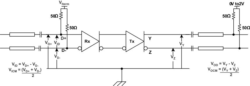 Figure 1. DisplayPort Sink Main Link Test Circuit
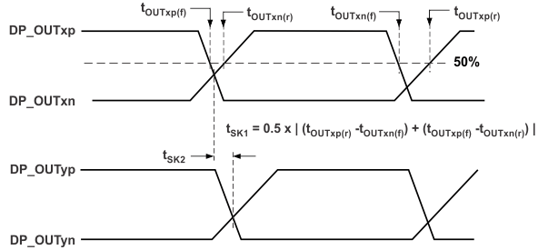 Figure 2. DisplayPort Sink Main Link Skew Measurements
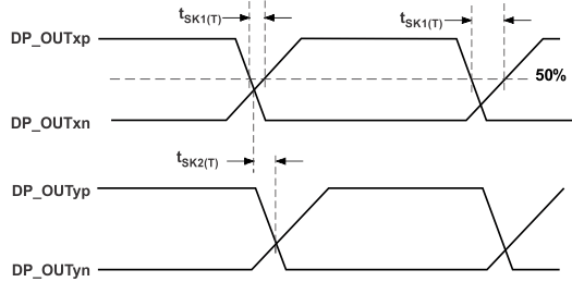 Figure 3. HDMI/DVI Sink TMDS Output Skew Measurements
 Figure 4. HDMI/DVI TMDS Output Common Mode Measurement
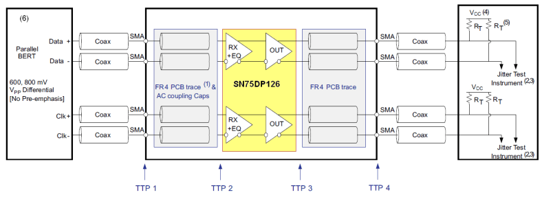
1. The FR4 trace between TTP1 and TTP2 is designed to emulate 1-8” of FR4, AC coupling cap and connector. Trace width –4 mils.
2. All Jitter is measured at a BER of 10-9
3. Residual jitter reflects the total jitter measured at TTP4 minus the jitter measured at TTP1
4. VCC = 3.3 V
5. RT = 50Ω
6. The input signal from parallel Bert does not have any pre-emphasis. Refer to recommended operating conditions.
Figure 5. HDMI/DVI TMDS Output Jitter Measurement
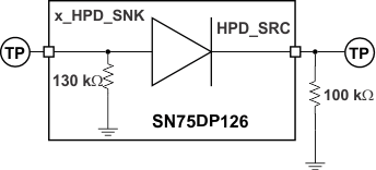 Figure 6. HPD Test Circuit
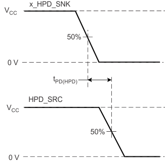 Figure 7. HPD Timing Diagram #1
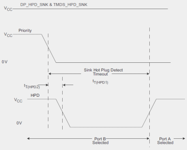 Figure 8. HPD Timing Diagram #2
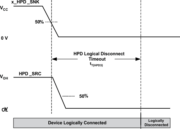 Figure 9. HPD Logic Disconnect Timeout
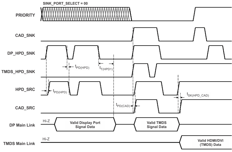 Figure 10. HPD and CAD Logic Description and Timing Diagram
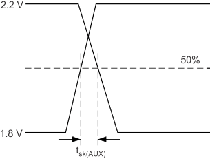 Figure 11. AUX Skew Measurement
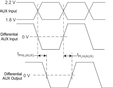 Figure 12. AUX Delay Measurement
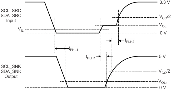 Figure 13. DDC Propagation Delay – Source to Sink
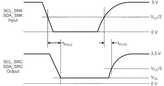 Figure 14. DDC Propagation Delay – Sink to Source
7.15 Typical Characteristics
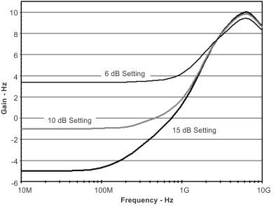
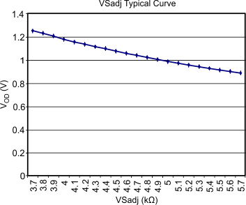
| Gain represents SN75DP126 design simulation. | ||
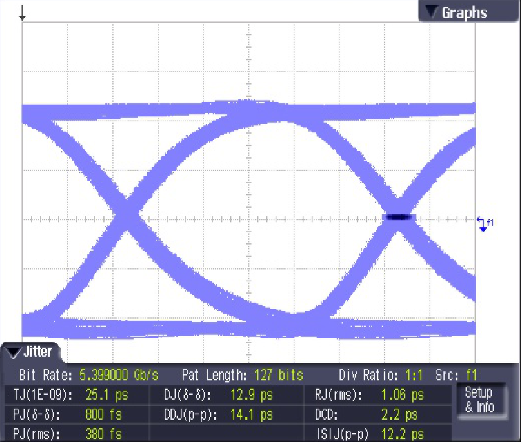
15 dB EQ Setting; DP Sink
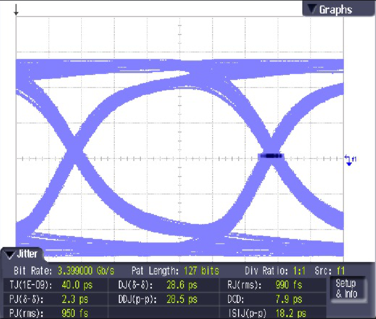
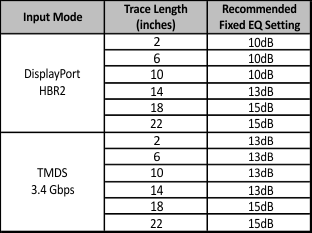
vs EQ Setting
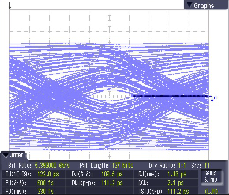
DisplayPort Sink
